As a veteran engineer at Zero One Solution Limited, with two decades of experience spanning Silicon Valley's tech landscape, I've witnessed firsthand the transformative power of innovation. Today, we stand on the cusp of an era where our homes are no longer just spaces, but intelligent ecosystems that anticipate our needs. This evolution is powered by sophisticated electronics, and at its heart lies the Printed Circuit Board (PCB). How can these complex systems be made reliable, efficient, and cost-effective? This article delves into the intricacies of smart home solutions, highlighting how Zero One Solution Limited's rapid-response R&D prototype manufacturing and one-stop PCB services are crucial in bringing these groundbreaking technologies to life, ensuring your smart home vision becomes a reality.
The Evolution of Smart Home Technology: From Science Fiction to Everyday Reality
The concept of smart homes, once confined to the realm of science fiction, has rapidly evolved into an integral part of modern living. This transformation, driven by the convergence of the Internet of Things (IoT), advanced connectivity, and declining costs of electronic components, has revolutionized how we interact with our living spaces. At the heart of this evolution lies the sophisticated interplay of electronic components, most notably Printed Circuit Boards (PCBs), which serve as the backbone for intelligent home automation systems.
The genesis of smart home technology can be traced back to early automation systems and remote controls. However, the true acceleration began with the proliferation of the internet and the development of wireless communication protocols. Technologies such as Wi-Fi, Bluetooth, and Zigbee enabled seamless connectivity between devices, paving the way for integrated smart home ecosystems. These advancements were further fueled by the miniaturization of electronic components, leading to the development of compact, efficient, and powerful smart home devices. As of 2023, the global smart home market was valued at USD 109.96 billion and is projected to reach USD 359.26 billion by 2030, growing at a CAGR of 18.35% from 2023 to 2030 (Source: Grand View Research).
The growing demand for intelligent home automation systems has significantly impacted daily life. From automated lighting and climate control to enhanced security systems and entertainment, smart home technologies offer unparalleled convenience, energy efficiency, and security. This has led to a shift in consumer expectations, with smart home features becoming increasingly desirable and, in some cases, essential. This widespread adoption is directly correlated with the advancements in underlying technologies, particularly in PCB design and manufacturing. Without robust and reliable PCBs, the vision of a seamlessly integrated smart home would remain unrealized.
In essence, the evolution of smart home technology is a testament to human ingenuity and technological progress. The transition from rudimentary automation to sophisticated, interconnected systems highlights the critical role of underlying electronic components like PCBs. As we move forward, the continuous advancements in PCB design, manufacturing, and assembly, such as those provided by Zero One Solution Limited, will be essential in driving further innovation and shaping the future of smart living.
Essential Hardware and Software Components Powering Smart Home Solutions
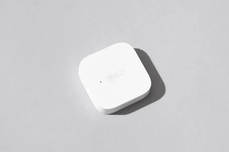
Smart Home Sensor Close-Up
At the heart of every smart home lies a carefully orchestrated ecosystem of hardware and software, working in concert to deliver intelligent automation and seamless user experiences. These components are interconnected, with custom PCB solutions acting as the critical backbone that enables their functionality and interaction. Understanding these core elements is crucial to appreciate the complexity and sophistication of modern smart home systems.
Sensors Sensors form the sensory organs of a smart home, collecting data about the environment. These can include motion sensors, door and window sensors, temperature and humidity sensors, and light sensors. Each sensor generates data that is processed to trigger actions, such as turning on lights or adjusting the thermostat. High-quality, reliable sensors are paramount, with the PCB design playing a key role in their performance and accuracy.
Actuators Actuators are the muscles of the smart home, executing commands based on sensor data or user input. Examples include smart switches, smart locks, motorized blinds, and smart thermostats. PCBs are essential in actuators, managing power distribution, signal processing, and communication, ultimately controlling physical devices within the home. Robust PCB design ensures the reliability and longevity of these critical components.
Communication Protocols Smart home devices communicate using a variety of wireless protocols. Wi-Fi provides broad coverage and is commonly used for connecting devices to the internet. Zigbee and Z-Wave offer low-power, mesh networking capabilities, ideal for battery-powered devices. Bluetooth is often used for short-range communication, such as connecting smartphones to smart speakers. The PCB design must accommodate the specific needs of each protocol, ensuring optimal signal integrity and minimal interference.
Central Hubs The central hub acts as the brain of the smart home, coordinating communication between devices, processing data, and providing a user interface for control. It connects to the home network and manages the various smart devices. The hub's PCB is a complex system that integrates multiple communication modules and processing units. Zero One Solution Limited's PCB services provide the design and manufacturing expertise to meet the demands of these advanced hubs.
Software and User Interfaces Software platforms manage the operation of smart home devices, offering features like automation, remote control, and data analysis. User interfaces, often in the form of mobile apps or voice assistants, provide intuitive control over the system. The software and user interface components rely heavily on robust hardware, where the PCB provides a platform for seamless integration. The quality of the PCB directly impacts the performance and responsiveness of the smart home system.
Zero One Solution Limited specializes in providing custom PCB solutions optimized for these core components, ensuring seamless integration, optimal performance, and enhanced user experience. Our expertise in rapid prototyping, design optimization, manufacturing, and assembly empowers our clients to build cutting-edge smart home solutions.
Overcoming Challenges in Smart Home Device Development Through Advanced PCB Solutions
The smart home revolution is transforming how we live, but its advancement hinges on overcoming significant technological hurdles. Developers face complex challenges in miniaturization, power efficiency, wireless interference, security, and interoperability. These issues directly impact the reliability, performance, and market viability of smart home devices. A robust PCB design and manufacturing strategy is essential to navigate these complexities successfully.
Here’s a detailed look at these challenges and the PCB solutions that address them:
Miniaturization and Compact Design: Smart home devices are increasingly expected to be small and discreet. This requires the use of High-Density Interconnect (HDI) PCBs, which enable more components to be packed into smaller spaces. The use of fine line spacing and microvias in HDI PCBs is critical to achieving compact designs without sacrificing functionality. Zero One Solution Limited specializes in HDI PCB manufacturing, enabling the creation of sleek, space-saving smart home gadgets.
Power Efficiency: Many smart home devices run on batteries or require low power consumption. This necessitates careful component selection and PCB layout to minimize power loss. Thermal management is also crucial; efficient heat dissipation prevents device overheating and prolongs battery life. Implementing power-saving modes and optimizing PCB traces for minimal resistance are important considerations that Zero One Solution Limited addresses through expert design and manufacturing practices.
Wireless Interference and Connectivity: Smart home devices rely heavily on wireless communication (Wi-Fi, Bluetooth, Zigbee). Wireless interference can disrupt connectivity and performance. To mitigate this, PCB design must consider impedance matching, signal integrity, and shielding techniques. Furthermore, antenna placement is crucial to ensure optimal signal strength. Zero One Solution Limited provides RF circuit design expertise to minimize interference and maximize the reliability of wireless connections.
Security Vulnerabilities: Protecting user data is paramount. Secure PCB design practices, including the use of secure boot mechanisms and tamper-resistant designs, are vital. Ensuring the use of robust components with built-in security features and rigorous testing of PCB designs against potential vulnerabilities are critical steps. Zero One Solution Limited's commitment to advanced security protocols ensures user data remains protected.
Interoperability Issues: Smart home devices from different manufacturers often need to work together seamlessly. This requires adherence to industry standards and careful PCB design to ensure compatibility. Testing and validation are key, and selecting components that support multiple communication protocols is crucial. Zero One Solution Limited is dedicated to ensuring designs are compatible with common smart home standards.
Addressing these challenges demands specialized PCB design, manufacturing, and assembly capabilities. By partnering with Zero One Solution Limited, smart home device developers gain access to cutting-edge PCB solutions, ensuring their products meet the stringent demands of this rapidly evolving market and achieve market success.
Zero One Solution Limited: Pioneering PCB Solutions for Smart Home Innovation
In the rapidly evolving smart home landscape, Zero One Solution Limited stands at the forefront, providing specialized PCB services tailored to meet the intricate demands of this innovative industry. Our expertise in rapid prototyping, design optimization, manufacturing, and assembly empowers smart home device manufacturers to accelerate their product development cycles and achieve faster time-to-market. As a strategic partner, we provide comprehensive PCB solutions that are critical for the seamless integration and optimal performance of smart home technologies.
Zero One Solution Limited’s one-stop solution approach streamlines the entire PCB lifecycle, from initial design to final assembly. This integrated strategy provides several key advantages:
Rapid Prototyping We offer fast-turnaround PCB prototyping services, allowing smart home device developers to quickly validate designs and iterate on product concepts. This accelerates the innovation process and ensures that products are market-ready sooner.
Design Optimization Our experienced engineering team provides expert design support, optimizing PCB layouts for performance, signal integrity, and manufacturability. This includes design for manufacturability (DFM) and design for assembly (DFA) checks to ensure efficient production and minimize potential issues.
Advanced Manufacturing We utilize advanced manufacturing techniques, including HDI, flexible PCBs, and RF circuit design, to meet the complex requirements of smart home devices. Our manufacturing capabilities support a wide range of form factors and functionalities, from compact sensors to sophisticated control panels.
Turnkey Assembly Services We provide full turnkey assembly services, including component sourcing, SMT (Surface Mount Technology) and through-hole assembly, and rigorous testing. This comprehensive approach reduces the complexity for our clients and ensures high-quality, reliable finished products.
Our commitment extends beyond providing exceptional services; we also contribute to the sustainability and efficiency of smart home solutions. By optimizing PCB designs for power efficiency and utilizing eco-friendly materials, we support our clients in creating environmentally responsible products. Zero One Solution Limited is dedicated to helping smart home innovators bring cutting-edge, reliable, and sustainable solutions to market.
Cutting-Edge PCB Technologies Powering the Smart Home Revolution
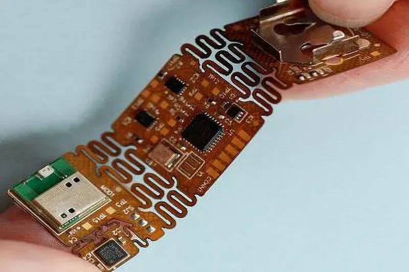
Flexible PCB
The rise of smart home technology is inextricably linked to advancements in Printed Circuit Board (PCB) technology. At Zero One Solution Limited, we recognize that the miniaturization, functionality, and reliability of smart home devices hinge on the sophistication of the PCBs they utilize. This section delves into the specific PCB technologies and manufacturing processes critical for enabling the innovative capabilities of smart home products, ensuring they meet the demands of today's connected living environments.
Here's a look at key PCB technologies and their applications:
High-Density Interconnect (HDI) PCBs HDI PCBs are essential for compact smart home devices such as smart sensors, thermostats, and door locks. Their ability to pack more components into smaller spaces facilitates the sleek designs and advanced functionality demanded by modern smart homes. At Zero One Solution Limited, our HDI PCB manufacturing capabilities ensure optimal performance in space-constrained applications, enabling the creation of unobtrusive and stylish smart home gadgets.
Flexible PCBs Flexible PCBs offer unparalleled design freedom, making them ideal for devices with unique form factors. They are particularly well-suited for wearable smart home devices, such as smart watches or flexible lighting strips. Zero One Solution Limited's expertise in flexible PCB manufacturing allows for the integration of smart technology into innovative, ergonomic designs, enhancing both functionality and aesthetics.
RF Circuit Design Reliable wireless communication is the backbone of any smart home. Optimized RF circuit design is crucial for ensuring seamless connectivity between devices. Our engineers at Zero One Solution Limited specialize in designing PCBs optimized for RF performance, including considerations for antenna placement, impedance matching, and signal integrity. This ensures robust and interference-free wireless communication within the smart home ecosystem, a critical factor for user satisfaction.
Advanced Materials The choice of PCB materials significantly impacts performance, especially in high-frequency applications. We use advanced materials with low dielectric loss and high thermal conductivity to create PCBs that excel in smart home devices. Our material selection process, including FR4, Rogers, and other specialized substrates, ensures the highest level of signal integrity and durability, key for a reliable smart home experience.
Surface Mount Technology (SMT) and Assembly Efficient and precise PCB assembly is crucial for realizing the full potential of smart home devices. Our state-of-the-art SMT lines at Zero One Solution Limited allow for the high-volume assembly of complex PCBs. We incorporate Automated Optical Inspection (AOI) and rigorous testing to maintain the highest quality standards, ensuring flawless performance and reliability of your smart home products.
By leveraging these advanced PCB technologies, Zero One Solution Limited empowers smart home innovators to create products that are not only technologically advanced but also reliable, efficient, and aesthetically pleasing. Our commitment to excellence in PCB design and manufacturing is a cornerstone of our support for the evolving smart home industry.
Securing Your Smart Home: Zero One Solution's Commitment to Reliability
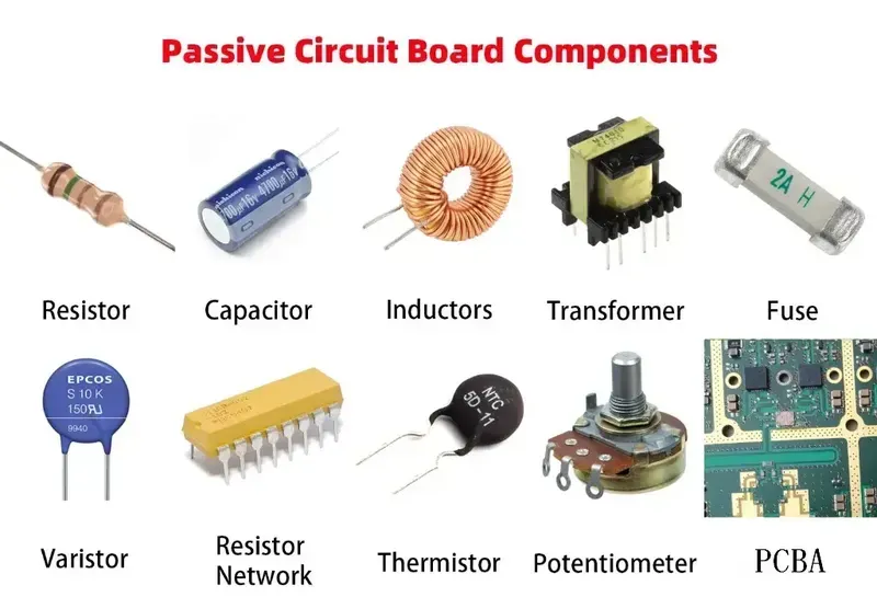
PCB component
In an increasingly interconnected world, the security and reliability of smart home devices are not just features, but fundamental requirements. With the proliferation of sensitive data and the potential for system vulnerabilities, safeguarding user information and ensuring consistent operation are critical. At Zero One Solution Limited, we place paramount importance on these aspects, integrating robust security measures and rigorous testing protocols into every PCB design and manufacturing process to build user trust and provide peace of mind.
Secure PCB Design Practices Our approach to secure PCB design starts at the component selection stage. We use components that are known for their security features, such as those with built-in encryption and secure boot capabilities. Following this, we implement design practices that minimize the attack surface. This includes:
* **Shielding:** Implementing shielding techniques to protect sensitive circuits from electromagnetic interference (EMI), which can be used for malicious purposes.
* **Trace Routing:** Careful trace routing to prevent signal leakage and cross-talk, further securing data transmission paths.
* **Secure Boot:** Implementing secure boot mechanisms that ensure only verified firmware is loaded, protecting against unauthorized software modifications.
Robust Component Selection We carefully select components that meet the stringent requirements of smart home applications. This includes using components that have undergone rigorous testing and certification, such as those certified by UL, CE, and other relevant industry standards. We partner with trusted component suppliers to source authentic parts and avoid counterfeit components that could compromise security and performance. We also consider the long-term availability and support of components to ensure the longevity of your smart home solutions.
Rigorous Testing Procedures Our commitment to reliability extends to thorough testing throughout the manufacturing process. We utilize:
* **Functional Testing:** Comprehensive functional testing to verify that all components and systems work as intended, simulating real-world conditions.
* **Environmental Testing:** Environmental testing to simulate the effects of temperature, humidity, and vibration on the PCB to ensure its reliability over time.
* **Security Audits:** Regular security audits to identify and address potential vulnerabilities in both hardware and firmware. These audits include penetration testing and vulnerability assessments to protect against cyber threats.
By adhering to these comprehensive security and reliability measures, Zero One Solution Limited ensures that our PCB solutions meet the highest standards of security and dependability, providing a solid foundation for your innovative smart home products. We are committed to delivering solutions that not only enhance user experience but also protect user data and ensure the longevity of your smart home investments.
The Future of Smart Home Solutions: Trends, Opportunities, and Zero One Solution's Role
The smart home sector is on the cusp of a significant transformation, driven by technological advancements and evolving consumer expectations. These advancements present compelling opportunities for innovation, and Zero One Solution Limited is strategically positioned to lead this evolution with cutting-edge PCB solutions. The future of smart homes is not just about automation; it's about creating intelligent, sustainable, and seamlessly integrated living spaces. This section explores emerging trends, future opportunities, and how Zero One Solution Limited is poised to support the next generation of smart living.
AI Integration and Personalized Automation Artificial Intelligence (AI) is poised to revolutionize smart home experiences. AI-powered systems will analyze user behavior, learn preferences, and proactively adjust home settings to optimize comfort, energy efficiency, and security. This integration requires sophisticated PCB designs that support high-speed data processing, machine learning algorithms, and complex sensor networks. Zero One Solution's expertise in high-density interconnect (HDI) PCBs and advanced RF circuit design is crucial for enabling these AI-driven smart home features.
Edge Computing for Enhanced Efficiency and Privacy Edge computing, which processes data closer to the source, is becoming increasingly important in smart homes. By reducing reliance on cloud-based processing, edge computing enhances responsiveness, reduces latency, and improves data privacy. This trend demands compact, power-efficient PCBs optimized for edge devices. Zero One Solution's rapid prototyping services and expertise in miniaturization enable the development of edge-computing-enabled smart home devices that offer superior performance and security.
Sustainable Smart Homes: Eco-Friendly Design Sustainability is a growing priority, and smart homes are at the forefront of this trend. Green building practices and energy-efficient appliances, controlled by smart home systems, contribute to reduced environmental impact and lower operating costs. This shift necessitates PCB designs that prioritize energy efficiency and the use of eco-friendly materials. Zero One Solution supports this trend by offering RoHS-compliant manufacturing and PCB designs optimized for low power consumption, contributing to the development of sustainable smart home solutions.
Enhanced Interoperability: The Matter Standard The lack of interoperability between smart home devices has been a significant barrier to widespread adoption. The Matter standard aims to solve this problem by providing a unified communication protocol, ensuring that devices from different manufacturers can seamlessly interact. This requires PCB designs that support multiple communication protocols (Wi-Fi, Thread, Bluetooth) and adhere to stringent interoperability requirements. Zero One Solution’s experience with diverse communication technologies makes us well-equipped to support the development of Matter-compliant devices.
The future of smart homes is dynamic, and Zero One Solution Limited is committed to staying at the forefront of innovation. By embracing emerging trends and offering cutting-edge PCB solutions, we empower our clients to create the next generation of smart home devices. Our focus on advanced PCB technologies, rapid prototyping, and reliable manufacturing ensures that our clients can bring their innovative products to market quickly and efficiently, shaping the future of smart living.
Frequently Asked Questions about Smart Home PCBs
Navigating the complexities of smart home technology often leads to specific inquiries about the underlying Printed Circuit Boards (PCBs). This section provides clear, concise answers to the most common questions, focusing on design, material selection, and layout optimization for peak performance in smart home devices. These insights are vital for developers and manufacturers looking to enhance device efficiency, reliability, and overall user experience.
What are the key design considerations for low-power smart home devices? Low-power smart home devices require careful PCB design to maximize battery life. Crucial considerations include choosing energy-efficient components, optimizing the PCB layout to minimize signal loss and power consumption, and employing power-saving modes. For example, using low-dropout regulators (LDOs) and implementing sleep modes can significantly extend the operational time of battery-powered devices. At Zero One Solution Limited, we specialize in designs that address these precise requirements, ensuring your devices operate efficiently.
How does material selection impact the wireless performance of PCBs in smart homes? The choice of PCB materials significantly affects wireless communication in smart home devices. Materials like FR-4, while cost-effective, may exhibit higher signal loss at high frequencies. For applications involving Wi-Fi, Bluetooth, or Zigbee, materials with lower dielectric constants and loss tangents, such as Rogers or high-frequency laminates, are preferable. These materials minimize signal attenuation, ensuring reliable wireless connectivity. Our expertise at Zero One Solution Limited includes selecting the right materials to optimize the performance of your wireless devices.
Why is PCB layout optimization important for compact smart home gadgets? Optimizing the PCB layout is essential for miniaturizing smart home gadgets while maintaining functionality. Effective layout strategies include component placement, trace routing, and signal integrity. Compact designs often use HDI (High-Density Interconnect) PCBs to accommodate more components in less space. At Zero One Solution Limited, our engineers are adept at employing these techniques to reduce device size, improve performance, and enhance the aesthetic appeal of your smart home products.
How can I ensure the security of my smart home device PCBs? Security in smart home devices is paramount, with the PCB playing a critical role. Implementing secure design practices includes using encrypted communication protocols, protecting sensitive data with tamper-proof designs, and adhering to industry security standards. Careful component selection is also essential, as vulnerabilities in components can compromise the entire system. Zero One Solution Limited incorporates robust security measures in our PCB designs, ensuring your devices are well-protected.
What testing and quality control measures are crucial for smart home PCBs? Rigorous testing and quality control (QC) are vital for reliable smart home PCBs. This includes automated optical inspection (AOI), in-circuit testing (ICT), and functional testing to verify performance and detect defects. At Zero One Solution Limited, we employ comprehensive QC procedures, including environmental stress testing, to ensure that every PCB meets stringent quality standards, guaranteeing long-term operational reliability in real-world conditions.
How does Zero One Solution Limited assist in optimizing the PCB design for smart home solutions? Zero One Solution Limited offers comprehensive services to optimize PCB designs for smart home applications. We provide expert design reviews, signal integrity analysis, thermal management solutions, and rapid prototyping to refine your designs. Our engineering team collaborates closely with clients, from initial concept to final production, ensuring optimal performance, efficiency, and manufacturability. Our one-stop solution accelerates product development and ensures market success for your smart home innovations.
The smart home revolution is not just a concept; it's a rapidly expanding reality driven by continuous innovation in electronics. Zero One Solution Limited, with its unwavering commitment to rapid prototyping and comprehensive PCB solutions, stands at the forefront of this transformation. Our expertise ensures that the complex interplay of sensors, processors, and communication modules within smart home devices is flawlessly executed, from concept to mass production. By choosing Zero One Solution Limited, you're not just getting a PCB provider; you're partnering with a team dedicated to accelerating your product development cycle and bringing cutting-edge smart home technologies to market with unparalleled efficiency and reliability. Ready to innovate your smart home product? Contact Zero One Solution Limited today and let's build the future, together.