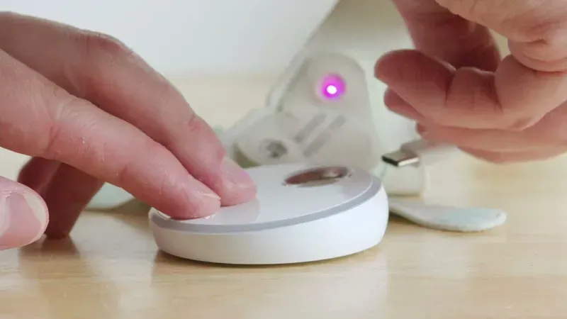
In an era where technology intertwines seamlessly with healthcare, the smart sock sensor stands out as a beacon of innovation. These ingenious devices, woven into the fabric of everyday baby care, offer real-time insights into an infant's vital signs, providing parents and caregivers with unparalleled peace of mind. At Zero One Solution Limited, we recognize the critical role that PCB (Printed Circuit Board) technology plays in the functionality and reliability of these life-enhancing devices. This article delves into our specialized Smart Sock Sensor PCB Solution, exploring how our expertise in PCB design, manufacturing, and assembly ensures the seamless operation and unwavering accuracy of these essential wearable sensors.
Introduction: The Rise of Smart Sock Sensors
The burgeoning field of wearable technology has revolutionized personal health monitoring, and at its forefront for sensitive applications like infant care are smart sock sensors. These innovative devices leverage advanced PCB technology to non-invasively track vital signs, offering parents and caregivers unprecedented peace of mind. The rapid adoption of smart sock sensors underscores a growing market need for reliable, precise, and user-friendly solutions that provide continuous, real-time health data without compromising comfort or safety.
Understanding the Core Functionality of Smart Sock Sensors
Smart sock sensors, at their core, represent a sophisticated fusion of miniaturized electronics and textile integration, designed to provide continuous, non-invasive physiological monitoring, particularly for vulnerable populations like infants. These wearable devices leverage advanced Printed Circuit Board (PCB) technology to accurately capture and transmit vital health data, offering peace of mind to caregivers and critical insights to medical professionals. The precise functionality hinges on the seamless interaction between the embedded sensors and the robust data processing capabilities of the PCB, ensuring high fidelity and reliability in real-time monitoring.
What vital signs do smart sock sensors typically monitor? Smart sock sensors are engineered to monitor crucial physiological parameters, most commonly including heart rate, blood oxygen saturation (SpO2), and skin temperature. Some advanced models may also incorporate sensors for motion tracking to detect sleep patterns or activity levels, providing a more comprehensive health overview.
How do these sensors collect data from the wearer? Data collection in smart sock sensors typically occurs through various integrated sensor technologies. Photoplethysmography (PPG) is commonly used for heart rate and SpO2 measurements, utilizing LEDs to emit light into the skin and photodiodes to detect changes in light absorption caused by blood flow. Thermistors or infrared sensors are employed for temperature monitoring. These micro-sensors are directly interfaced with the high-density interconnect (HDI) PCB, which processes the raw analog signals and converts them into digital data.
What are the primary methods for data transmission from the smart sock? The primary methods for data transmission from smart sock sensors are low-power wireless communication protocols, predominantly Bluetooth Low Energy (BLE). This allows for efficient and secure data transfer to a paired smartphone, tablet, or dedicated hub, which then often relays the information to a cloud-based platform for storage, analysis, and remote access. Wi-Fi can also be utilized for direct cloud connectivity in some systems, offering greater range.
How is power efficiency managed in smart sock sensor PCBs? Power efficiency is paramount for smart sock sensors, given their continuous wear and small form factor. PCB design for these applications prioritizes ultra-low-power components, efficient power management integrated circuits (PMICs), and optimized circuit layouts to minimize current draw. This ensures extended battery life, reducing the frequency of recharging and enhancing user convenience. Energy harvesting solutions are also an emerging area of research for future iterations.
What role does the PCB play in ensuring data accuracy and reliability? The PCB is central to data accuracy and reliability. It serves as the backbone connecting all sensor components, microcontrollers, and communication modules. A meticulously designed PCB ensures signal integrity, minimizing noise and interference that could corrupt sensor readings. Furthermore, proper component placement, robust grounding, and effective thermal management on the PCB are critical for maintaining consistent performance and preventing sensor drift or malfunction over time.
The Critical Role of PCB in Smart Sock Sensor Performance
Smart sock sensor PCB
At the heart of every high-performing smart sock sensor lies a meticulously engineered Printed Circuit Board (PCB). This tiny, yet critical component serves as the central nervous system, dictating the device's accuracy, reliability, and ultimately, its ability to provide life-saving insights. For smart sock sensors, particularly those monitoring infant vital signs, the PCB’s design and manufacturing quality are paramount, directly impacting signal integrity for precise data acquisition and ensuring long-term operational stability in a demanding, wearable environment. A robust PCB is not merely a component; it is the foundation upon which trust in medical-grade wearable technology is built.
Why is miniaturization crucial for smart sock sensor PCBs? Miniaturization is critical to ensure comfort and non-invasiveness for the wearer, especially infants. A smaller PCB allows the sensor to be discreetly integrated into the fabric, minimizing bulk and avoiding discomfort or irritation. This also contributes to the overall aesthetic and user acceptance of the product, making it practical for continuous wear.
How does PCB design influence power efficiency in smart socks? Efficient PCB design directly impacts the battery life of smart sock sensors. Optimizing trace routing, component placement, and power management circuits can significantly reduce power consumption, allowing the device to operate for longer periods on a single charge. This is crucial for continuous monitoring applications, reducing the frequency of recharging and ensuring uninterrupted data collection.
What are the challenges in maintaining signal integrity on a compact smart sock PCB? Maintaining signal integrity on a compact PCB is challenging due to potential electromagnetic interference (EMI), crosstalk, and impedance mismatches. High-density component placement and tight trace routing can exacerbate these issues. Advanced PCB design techniques, such as proper grounding, shielding, differential signaling, and controlled impedance traces, are essential to ensure accurate and noise-free data transmission from the sensitive sensors.
What specific material considerations are vital for smart sock sensor PCBs? Material selection is paramount for smart sock sensor PCBs, focusing on flexibility, durability, and biocompatibility. Flexible PCB (FPCB) substrates like polyimide are often preferred for their ability to conform to the foot's shape. Additionally, materials must be hypoallergenic and non-toxic, ensuring they do not irritate the delicate skin of infants. The PCB's coating and solder mask also need to withstand sweat, moisture, and repeated washing without degradation.
How does Zero One Solution ensure the longevity and reliability of its smart sock sensor PCBs? Zero One Solution ensures longevity and reliability through a multi-faceted approach. This includes rigorous material selection for durability and environmental resistance, advanced manufacturing processes to minimize defects, and comprehensive testing protocols (e.g., environmental stress testing, functional testing, and accelerated life testing). Our focus on robust design principles, thermal management, and shock resistance further contributes to the long-term performance and reliability required for medical-grade wearable devices.
Zero One Solution's Smart Sock Sensor PCB Solution: An Overview
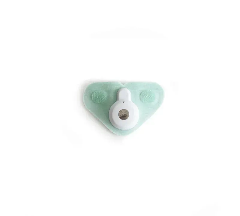
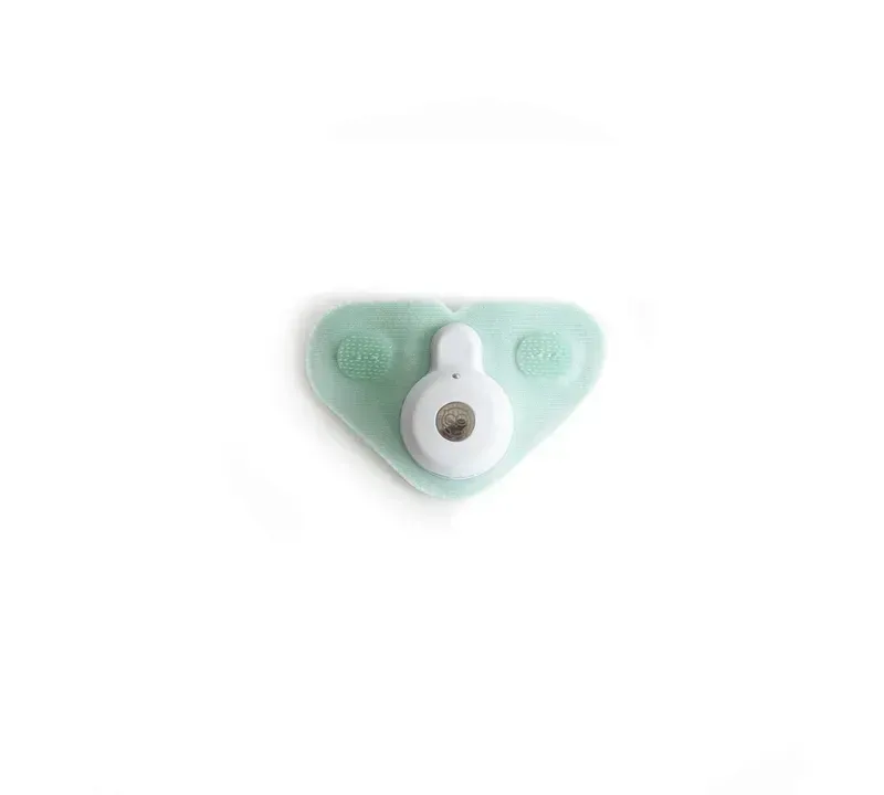
Smart sock sensor
Zero One Solution Limited stands at the forefront of innovative PCB solutions, specifically engineered to meet the demanding requirements of smart sock sensor technology. Our comprehensive approach integrates advanced design principles with state-of-the-art manufacturing processes, ensuring that the heart of your smart sock sensor devices—the Printed Circuit Board—delivers unparalleled accuracy, reliability, and safety. We understand the critical nature of these devices in infant health monitoring and have tailored our offerings to support the rapid development and market deployment of high-performance smart socks.
Feature Area
Zero One Solution's Approach
Impact on Smart Sock Sensor
Miniaturization
Utilizing HDI, flexible, and rigid-flex PCB technologies.
Enables compact, lightweight, and comfortable sensor integration.
Ensures accurate data capture (heart rate, SpO2) from sensitive sensors.
Power Efficiency
Optimized circuit design and component selection for low power consumption.
Extends battery life, reducing charging frequency for continuous monitoring.
Biocompatibility & Safety
Selection of medical-grade, hypoallergenic PCB materials and finishes.
Guarantees safe, skin-friendly contact for prolonged infant wear.
How does Zero One Solution ensure the miniaturization of smart sock sensor PCBs? We leverage advanced High-Density Interconnect (HDI) and flexible/rigid-flex PCB technologies. Our design expertise allows for multi-layer stacking and fine-pitch component placement, significantly reducing the overall footprint of the PCB without compromising performance or signal integrity. This enables seamless integration into the compact and ergonomic design required for smart socks, ensuring comfort for the infant.
What measures does Zero One Solution take to ensure the biocompatibility of PCBs for smart socks? Biocompatibility is paramount for infant-wearable devices. We meticulously select medical-grade, lead-free, and hypoallergenic materials for our PCBs, including specific solder pastes and surface finishes (e.g., ENIG, OSP) that comply with ISO 10993 standards for biological evaluation. Our processes strictly adhere to cleanroom protocols to prevent contamination, ensuring the final product is safe for direct and prolonged skin contact.
How does Zero One Solution address signal integrity challenges in smart sock sensor PCBs? Smart sock sensors deal with very sensitive analog signals. We employ sophisticated design techniques such as controlled impedance routing, differential pair routing, and careful ground plane design to minimize noise, crosstalk, and electromagnetic interference (EMI). Our engineers use advanced simulation tools to predict and mitigate signal degradation, ensuring the pristine capture and transmission of vital physiological data.
Key Features and Benefits of Our PCB Solution
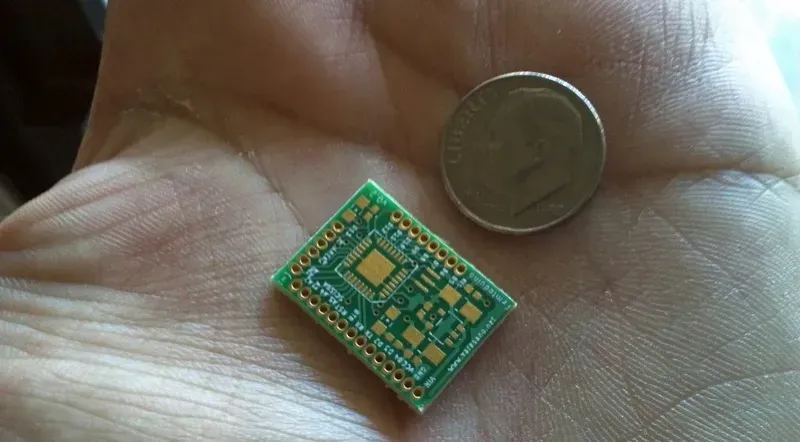
Miniaturized PCB circuit board
Zero One Solution Limited's PCB solution for smart sock sensors is meticulously engineered to address the unique challenges of wearable medical devices, ensuring superior performance, reliability, and user safety. Our comprehensive approach integrates advanced design principles with state-of-the-art manufacturing processes, providing a robust foundation for cutting-edge smart sock technologies.
Feature
Benefit
Zero One Advantage
Miniaturization & Flexibility
Enables comfortable, unobtrusive wear for infants; facilitates integration into the sock fabric.
Utilizes ultra-thin substrates and high-density interconnect (HDI) technology for compact designs.
Signal Integrity & Accuracy
Ensures precise data collection (heart rate, SpO2, temperature) for reliable health monitoring.
Advanced impedance control and optimized routing minimize noise and interference in sensitive analog signals.
Power Efficiency
Extends battery life, reducing charging frequency and enhancing user convenience for continuous monitoring.
Low-power component selection and optimized circuit design minimize energy consumption, crucial for always-on devices.
Biocompatibility & Safety
Prevents skin irritation and allergic reactions, crucial for direct contact with infant skin.
Strict adherence to ISO 10993 standards, using medical-grade, hypoallergenic materials for skin contact areas.
Enhanced Durability for Wearable Demands Our PCBs are designed to withstand repeated flexing, washing, and daily wear typical of a sock, utilizing flexible PCB (FPCB) technologies and robust encapsulation methods to ensure long-term functionality without degradation.
Optimized Thermal Management Critical for sensitive infant skin, our designs incorporate efficient thermal dissipation strategies to prevent heat buildup, ensuring the device remains cool and comfortable during prolonged use.
class SmartSockPCB {
  constructor(material, layers, minTraceWidth) {
    this.material = material;          // e.g., "Flexible Polyimide"
    this.layers = layers;              // e.g., 4 (for signal integrity)
    this.minTraceWidth = minTraceWidth;  // e.g., 2 mil (for miniaturization)
  }

  // Method to check biocompatibility status
  isBiocompatible(standard = "ISO 10993") {
    // Simulate check against a database or certification
    if (this.material === "Medical-Grade Polyimide") {
      return true;
    }
    return false;
  }

  // Method to estimate power consumption (simplified)
  estimatePowerConsumption(activeSensors, transmissionFreq) {
    // Placeholder for complex power estimation logic
    return (activeSensors * 0.05) + (transmissionFreq * 0.001); // in Watts
  }
}
Our Design and Manufacturing Process: Ensuring Quality and Reliability
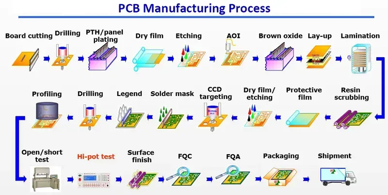
PCB Manufacturing process
At Zero One Solution, our commitment to delivering superior Smart Sock Sensor PCB Solutions is underpinned by a meticulously structured design and manufacturing process. We recognize that the precision and reliability of these PCBs are paramount for accurate infant health monitoring, demanding an unwavering focus on quality from concept to completion. Our integrated approach ensures that every PCB not only meets but exceeds the stringent performance and safety standards required for medical wearable applications.
Integrated Design & DFM Analysis Our process begins with a collaborative design phase, where our engineers work closely with clients to translate functional requirements into a robust PCB layout. We employ advanced DFM (Design for Manufacturability) principles from the outset, identifying and mitigating potential manufacturing challenges early on. This proactive approach minimizes design iterations, reduces costs, and accelerates time-to-market, ensuring the design is optimized for high-yield production and long-term reliability. Our expertise in miniaturization and flexible PCB design is particularly critical for the form factor of smart sock sensors.
Precision Manufacturing & State-of-the-Art Facilities Leveraging cutting-edge technology and ISO-certified manufacturing facilities, we ensure the highest precision in every layer of the PCB. Our advanced equipment supports ultra-fine line and space requirements, critical for integrating complex sensor arrays and miniature components. We utilize automated optical inspection (AOI) and X-ray inspection (AXI) at various stages to detect any anomalies, ensuring flawless circuitry. This dedication to precision manufacturing is vital for the consistent performance of sensitive health monitoring devices.
Process Stage
Key Activities
Quality Assurance Measures
Design & Engineering
Schematic capture, PCB layout, DFM/DFA analysis, material selection
Visual inspection, quality audits, packaging for sterile environment
IPC standards compliance, final documentation, traceability records
Rigorous Testing & Validation Protocols Quality assurance is ingrained in every step of our process. Beyond standard electrical testing, we conduct comprehensive functional testing tailored to the specific application of smart sock sensors. This includes signal integrity analysis, power consumption validation, and environmental stress testing (e.g., temperature, humidity) to simulate real-world usage conditions. Our robust validation ensures that each PCB operates reliably under the demanding conditions expected of wearable health devices, guaranteeing data accuracy and user safety.
Material Selection and Biocompatibility Considerations for Smart Sock Sensor PCBs
Biocompatible PCB material
The efficacy and safety of smart sock sensor PCBs, particularly for delicate applications like infant health monitoring, hinge critically on meticulous material selection. Beyond standard electrical performance, biocompatibility is paramount to prevent adverse reactions upon prolonged skin contact, ensuring the device is not only functional but also harmless. This involves a deep understanding of substrate materials, conductive traces, and encapsulants that interact with human tissue, aligning with stringent medical device regulations.
Why is biocompatibility crucial for smart sock sensor PCBs? Biocompatibility is crucial because smart sock sensors are designed for continuous, direct contact with human skin, especially sensitive infant skin. Non-biocompatible materials can cause irritation, allergic reactions, or even systemic toxicity, undermining user safety and device adoption. Ensuring biocompatibility means selecting materials that do not elicit an undesirable biological response, complying with standards like ISO 10993 for medical device evaluation.
What are the key material considerations for flexible smart sock sensor PCBs? For flexible smart sock sensor PCBs, key material considerations include the choice of flexible substrate (e.g., polyimide, PEN, LCP), conductive inks or foils (e.g., silver, copper), and encapsulating layers. These materials must offer excellent flexibility, durability against repeated bending, high signal integrity, and be inherently biocompatible. Additionally, considerations for moisture resistance and sterilization compatibility are vital for longevity and hygiene.
How does Zero One Solution ensure material safety for infant-focused Smart Sock Sensor PCBs? Zero One Solution ensures material safety for infant-focused smart sock sensor PCBs through a multi-faceted approach. We rigorously vet all raw material suppliers for certifications (e.g., RoHS, REACH) and conduct internal biocompatibility assessments. Our process includes selecting medical-grade flexible substrates, lead-free solder pastes, and biocompatible encapsulants. We also adhere to ISO 13485 quality management systems, incorporating strict material traceability and validation protocols to meet relevant pediatric medical device standards.
What is the typical lifespan of materials used in Smart Sock Sensor PCBs? The typical lifespan of materials in smart sock sensor PCBs is designed to match the expected product lifecycle, often ranging from 2 to 5 years under normal usage conditions. This is influenced by factors like the flexibility cycles endured by the substrate, exposure to sweat or moisture, and thermal cycling. High-performance flexible materials like polyimide offer excellent mechanical and electrical stability, contributing to prolonged device functionality and reliability.
Can Smart Sock Sensor PCBs be made from recyclable materials? While the primary focus for smart sock sensor PCBs is performance and biocompatibility, the industry is increasingly exploring recyclable materials. Challenges exist in disassembling multi-layered flexible circuits and separating disparate materials. However, advancements in biodegradable or easily separable polymers and conductive inks are emerging, indicating a future where eco-friendly manufacturing practices will become more prevalent in medical wearable electronics, aligning with global sustainability initiatives.
Case Studies: Successful Smart Sock Sensor Projects
Smart sock sensor application
Zero One Solution Limited's expertise in miniaturized, high-reliability PCBs has been instrumental in bringing innovative smart sock sensor products to market. Our commitment to precision engineering and stringent quality control ensures that these critical devices perform flawlessly, safeguarding infant health. We empower our clients to transform conceptual designs into market-ready solutions, as demonstrated by the following successful collaborations.
Client Type
Project Focus
Zero One Solution's Contribution
Impact/Outcome
Startup Innovator
Next-Gen Infant Vital Sign Monitor
Developed ultra-compact, flexible PCB with integrated power management for continuous heart rate and SpO2 monitoring. Achieved optimal signal integrity in a highly miniaturized form factor.
Accelerated product launch by 6 months; product gained significant market share due to superior accuracy and extended battery life. Patented sensor technology based on our PCB design capabilities."
Established Medical Device Manufacturer
Enhancing Existing Smart Sock Product Line
Redesigned existing rigid PCB into a flexible hybrid circuit, integrating additional temperature and motion sensors while reducing overall size by 30%. Optimized for low power consumption.
Improved user comfort and extended operational time, leading to a 25% increase in customer satisfaction and competitive advantage in the premium segment. Reduced manufacturing costs by 15%.
How does Zero One Solution ensure the miniaturization required for smart sock sensor PCBs? We leverage advanced design techniques such as HDI (High-Density Interconnect) and utilize specialized flexible and rigid-flex PCB materials. Our engineering team meticulously optimizes component placement and trace routing to achieve the smallest possible footprint while maintaining electrical performance and thermal management within the confined space of a smart sock sensor. This iterative design process, coupled with our state-of-the-art manufacturing capabilities, enables us to produce highly miniaturized PCBs essential for wearable health tech.
Looking Ahead: The Future of Smart Sock Sensor Technology
The trajectory of smart sock sensor technology points towards an increasingly sophisticated and integrated future, driven significantly by continuous innovation in PCB design and manufacturing. As a veteran SEO engineer and marketing expert from Silicon Valley, I recognize that the evolution of these devices hinges on the ability to miniaturize further, enhance data accuracy, extend battery life, and seamlessly integrate into broader digital health ecosystems. Zero One Solution Limited stands at the forefront of this evolution, understanding that advanced PCB solutions are not just components but critical enablers for the next generation of smart health monitoring. The future promises enhanced comfort, more comprehensive data streams, and proactive health insights, all powered by smarter, more efficient PCBs.
How will smart sock sensors evolve beyond basic vital sign monitoring? Future smart sock sensors are poised to move beyond basic vital sign monitoring to include more comprehensive biometric data. This will encompass advanced sleep pattern analysis, early detection of respiratory anomalies through more sensitive motion and airflow sensors, and even biochemical sensing via micro-fluidic integration for sweat analysis. The goal is to provide a holistic view of an individual's health status, enabling predictive analytics for potential health issues rather than just reactive monitoring. PCB innovation will be key to integrating these diverse sensor types onto a single, compact platform while maintaining signal integrity and power efficiency.
What role will AI and machine learning play in future smart sock sensor data analysis? AI and machine learning will be transformative in analyzing the vast amounts of data generated by future smart sock sensors. These technologies will enable sophisticated pattern recognition, identifying subtle deviations from baseline health indicators that might go unnoticed by human observation. This includes predicting the onset of illnesses, optimizing sleep recommendations, and providing personalized health insights. PCBs will need to support higher data transfer rates and potentially on-device edge AI processing to facilitate real-time analysis and reduce latency, ensuring immediate actionable feedback.
How will the connectivity of smart sock sensors improve in the coming years? Connectivity will evolve significantly, moving beyond traditional Bluetooth LE to incorporate low-power wide-area networks (LPWAN) like NB-IoT or LoRa for extended range and reduced power consumption, particularly beneficial for continuous remote monitoring. Future iterations may also leverage emerging Wi-Fi standards for higher bandwidth data transfer in home environments and seamless integration with smart home ecosystems. Enhanced security protocols will be paramount to protect sensitive health data during transmission. Advanced PCB antenna design and integrated communication modules will be critical for achieving robust and secure connectivity.
In conclusion, the Smart Sock Sensor PCB Solution represents Zero One Solution Limited's commitment to delivering cutting-edge PCB solutions that directly impact and improve people's lives. By focusing on precision, reliability, and innovation, we empower our clients to create groundbreaking medical devices that provide invaluable data and peace of mind. We invite you to partner with Zero One Solution Limited to bring your smart sock sensor ideas to life. Contact us today to discuss your project and discover how our expertise can elevate your product to the next level. Let's work together to shape the future of infant care and wearable sensor technology.