Soil pollution poses a significant threat to our ecosystems and human health. Effective monitoring is crucial for identifying and mitigating contaminated areas. Printed Circuit Boards (PCBs) play a vital role in environmental monitoring equipment, providing the necessary electronic infrastructure for sensors and data acquisition systems. In this article, we will explore how Zero One Solution Limited's PCB solutions are contributing to advancements in soil pollution monitoring, enabling more accurate and efficient detection of pollutants. How can specialized PCB design improve the accuracy and reliability of soil pollution detection devices?
The Growing Need for Soil Pollution Monitoring
Soil pollution, a silent yet pervasive threat, is escalating globally, compromising the very foundation of our ecosystems and human well-being. From industrial discharge to agricultural runoff, contaminants like heavy metals, pesticides, and persistent organic pollutants infiltrate soil, leading to significant detrimental effects on agriculture through reduced crop yields and compromised food safety, impacting water resources by leaching into groundwater, and posing direct risks to human health through the food chain and direct exposure. The urgency for accurate and reliable soil pollution monitoring techniques has never been greater, as proactive identification and assessment are crucial for effective remediation and safeguarding future generations.
Pollutant Category
Examples
Key Impacts
Heavy Metals
Lead, Cadmium, Mercury, Arsenic
Reduced crop vitality, bioaccumulation in food chain, neurological damage
Pesticides & Herbicides
DDT, Atrazine, Glyphosate
Disruption of soil microbiome, water contamination, endocrine disruption
Persistent Organic Pollutants (POPs)
PCBs, Dioxins, Furans
Long-term environmental persistence, carcinogenicity, immune system suppression
Why is soil pollution a growing global concern? Soil pollution is escalating due to intensified industrialization, urbanization, and agricultural practices, leading to a build-up of harmful contaminants. This poses a severe threat to food security, water quality, and human health, making its monitoring and mitigation a critical global agenda. According to a 2021 report by the Food and Agriculture Organization (FAO) of the United Nations, a significant percentage of global agricultural land is impacted by various forms of degradation, including chemical contamination, directly affecting food production and safety standards worldwide. This underscores the scale of the problem and the necessity for robust monitoring solutions to safeguard agricultural productivity and public health.
The Role of PCBs in Environmental Monitoring Equipment
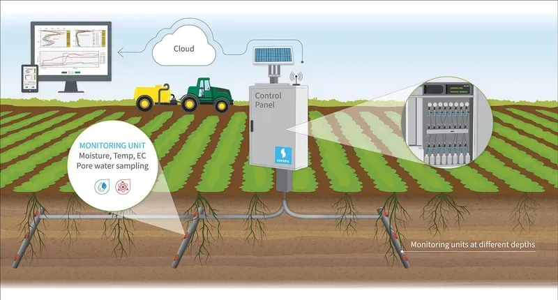
Soil Pollution Monitoring Equipment
Printed Circuit Boards (PCBs) are the indispensable backbone of modern soil pollution monitoring equipment, providing the foundational platform for integrating complex electronic components. These sophisticated devices, ranging from portable field kits to stationary sensor networks, rely on PCBs to seamlessly connect sensors, microcontrollers, data acquisition modules, and communication systems. The precise design and robust construction of PCBs directly dictate the accuracy, reliability, and longevity of environmental monitoring solutions, enabling real-time data collection and analysis critical for effective soil health management.
Key Functions of PCBs in Monitoring Devices PCBs serve as the central nervous system, facilitating signal routing, power distribution, and component integration. They are essential for sensor interfacing, analog-to-digital conversion, data processing, and wireless communication, ensuring that raw environmental data is accurately captured and transmitted for analysis.
Durability and Environmental Resilience Given the harsh and varied environments in which soil monitoring equipment operates, PCBs must exhibit exceptional durability. This includes resistance to moisture, temperature fluctuations, dust, and chemical exposure. Specialized coatings, robust material selection, and conformal finishes are often employed to protect the circuitry and ensure continuous operation.
Precision and Signal Integrity Accurate soil pollution measurement demands high signal integrity from the PCB. The design must minimize noise interference and crosstalk, especially for sensitive analog signals from chemical or biological sensors. Careful trace routing, grounding strategies, and component placement are crucial to maintain measurement precision and data fidelity.
Power Efficiency for Remote Deployment Many soil pollution monitoring systems are deployed in remote locations, relying on battery power or solar energy. PCBs are designed with power efficiency in mind, optimizing component selection and circuit layout to minimize consumption. This extends operational periods and reduces maintenance requirements, critical for long-term monitoring.
Integration of Communication Modules Effective monitoring requires data transmission. PCBs integrate various communication modules such as Wi-Fi, LoRa, cellular (2G/3G/4G/5G), and satellite links. The PCB design must accommodate the specific RF requirements of these modules, ensuring stable and reliable data transfer from the field to central monitoring stations or cloud platforms.
PCB Characteristic
Impact on Soil Monitoring Equipment
Benefit for Environmental Scientists
High Signal Integrity
Accurate sensor readings for pollutants (e.g., heavy metals, pesticides)
Reliable data for precise environmental assessments and remediation planning
Robustness & Durability
Resistance to harsh outdoor conditions (moisture, temperature extremes)
Extended operational lifespan and reduced maintenance in field deployments
Low Power Consumption
Longer battery life for remote, autonomous systems
Enables continuous monitoring in off-grid locations without frequent intervention
Compact Size & Miniaturization
Smaller, more portable and discreet monitoring devices
Easier deployment in diverse terrains and less visual impact
Interference Shielding
Minimizes electrical noise affecting sensor data
Ensures the validity and reliability of collected pollution data
Zero One Solution's PCB Design Expertise for Soil Monitoring
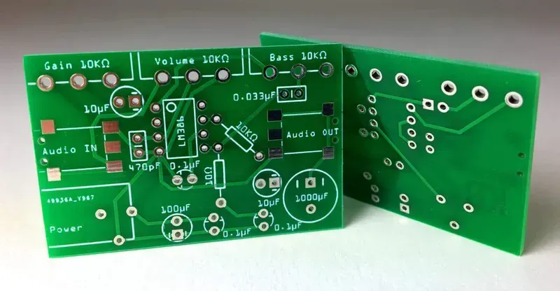
PCB Board Design for Environmental Monitoring
Zero One Solution Limited stands at the forefront of PCB design, offering specialized expertise crucial for the rigorous demands of soil pollution monitoring equipment. Our deep understanding of environmental sensing applications allows us to engineer PCBs that are not only robust and reliable but also precisely optimized for superior performance. We focus on critical design considerations such as maintaining impeccable signal integrity, minimizing noise interference, and achieving exceptional power efficiency, all of which are paramount for accurate and continuous environmental data acquisition.
Design Consideration
Importance for Soil Monitoring PCBs
Zero One Solution's Approach
Signal Integrity
Ensures accurate transmission of minute sensor data without degradation, vital for detecting low concentrations of pollutants.
Advanced routing techniques, impedance matching, and material selection to preserve signal fidelity, even in challenging environments and for sensitive analog signals from various sensors (e.g., pH, conductivity, heavy metals).
Low Noise Design
Prevents erroneous readings from environmental or electrical interference, providing clean data for precise analysis of soil parameters.
Implementation of shielding, proper grounding strategies, and component placement to minimize electromagnetic interference (EMI) and cross-talk, crucial for maintaining the accuracy of highly sensitive electrochemical sensors and optical sensors used in soil analysis systems, which often operate with very low voltage signals that are susceptible to noise.
Optimized Power Efficiency Critical for remote and battery-powered soil monitoring units, our designs reduce energy consumption, extending operational lifespans and minimizing maintenance. This involves selecting low-power components and implementing intelligent power management circuits to maximize battery life, especially important for devices deployed in remote agricultural or environmental sites where frequent battery replacement is impractical or costly.
Durability & Environmental Resilience PCBs for soil monitoring must withstand harsh outdoor conditions, including temperature extremes, humidity, and potential chemical exposure. We utilize robust materials, conformal coatings, and advanced encapsulation techniques to ensure long-term reliability and performance in the field, safeguarding against moisture, dust, and corrosive elements, which can significantly degrade standard PCBs.
Miniaturization for Compact Devices As monitoring devices become smaller and more portable, our expertise in high-density interconnect (HDI) and compact PCB layouts is essential. This allows for the integration of more functionality into smaller footprints, facilitating easier deployment and less intrusive monitoring in diverse terrains, while maintaining optimal performance. Our designs often incorporate fine-pitch components and multi-layer boards to achieve the required density without compromising signal integrity or thermal management.
Rapid Prototyping for Accelerated Development of Soil Pollution Monitoring PCB Solutions
PCB Prototype for Soil Monitoring
In the critical field of soil pollution monitoring, where timely and accurate data is paramount for environmental protection and public health, the ability to rapidly iterate and refine hardware designs is a significant competitive advantage. Zero One Solution Limited's rapid prototyping services are specifically engineered to accelerate the development cycle of complex PCB solutions for soil monitoring equipment, transforming conceptual designs into functional prototypes with unprecedented speed and precision. This agile approach minimizes time-to-market, allowing for swift validation of design integrity and performance in real-world conditions, ultimately enhancing the efficacy and reliability of environmental monitoring technologies.
Expedited Design Validation Rapid prototyping allows engineers to quickly test PCB designs, identify potential flaws, and validate performance parameters in a functional environment, significantly reducing the risk of costly rework in later stages. This is crucial for sensor-driven soil monitoring systems where signal integrity and power efficiency are paramount.
Optimized Iteration Cycles Our streamlined rapid prototyping process facilitates multiple design iterations within a short timeframe. This iterative approach enables continuous improvement of PCB layouts, component selection, and overall system integration, leading to more robust and reliable soil monitoring devices. Each cycle brings the design closer to an optimal solution, addressing real-world challenges proactively.
Manufacturing and Assembly Excellence
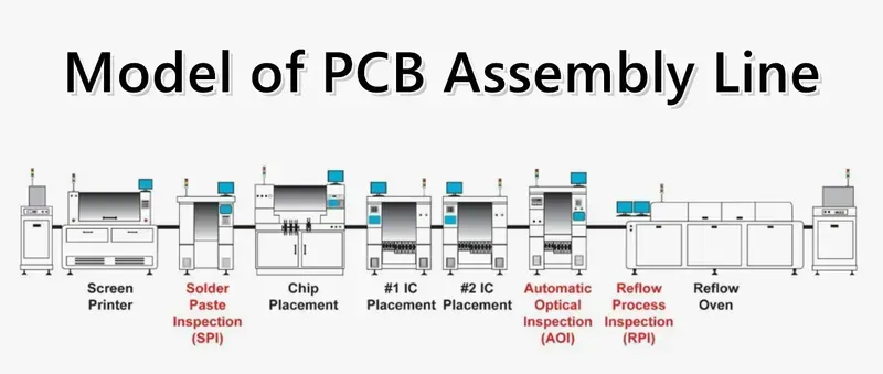
PCB Assembly Line
Zero One Solution Limited's commitment to manufacturing and assembly excellence is paramount in delivering robust PCB solutions for critical applications like soil pollution monitoring. Our state-of-the-art facilities and rigorous processes ensure that every board produced meets the highest standards of quality and reliability, capable of withstanding the challenging conditions often encountered in environmental sensing deployments. This unwavering dedication translates directly into the dependable performance of your monitoring equipment, providing accurate and consistent data essential for environmental protection.
Aspect
Description
Benefit for Soil Monitoring PCBs
Automated Assembly Lines
Utilizing advanced pick-and-place machines and reflow ovens for precise component placement and soldering.
Ensures high accuracy and repeatability, reducing errors critical for sensitive sensor circuits.
Rigorous Quality Control
Multi-stage inspection process including Automated Optical Inspection (AOI), X-ray inspection, and in-circuit testing (ICT).
Guarantees defect-free boards, enhancing the longevity and reliability of field-deployed monitoring devices.
Material Sourcing & Traceability
Partnerships with certified suppliers and comprehensive material traceability systems.
Ensures consistent material quality, crucial for environmental durability and sensor performance.
Environmental Compliance
Adherence to industry standards such as RoHS and REACH, promoting sustainable manufacturing practices.
Supports the environmental objectives of soil pollution monitoring projects by minimizing hazardous substances.
IPC Standards Adherence
Manufacturing processes strictly follow IPC-A-610 and IPC-6012 standards for electronics manufacturing.
Provides a benchmark for quality and reliability, ensuring PCBs are robust enough for harsh outdoor conditions.
Case Studies: Successful Soil Monitoring PCB Applications
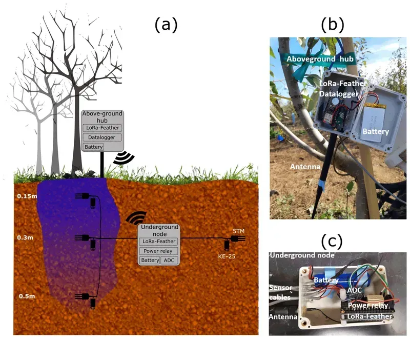
Soil Monitoring Case Study
Zero One Solution Limited's commitment to precision engineering and rapid prototyping has led to the successful deployment of our PCB solutions in numerous critical soil pollution monitoring applications. These real-world case studies underscore the tangible benefits our advanced PCBs bring to environmental protection, enabling more accurate, reliable, and efficient detection of contaminants.
Project Name
Challenge Addressed
Zero One Solution's PCB Impact
Quantifiable Improvement
Agricultural Land Contamination Sensing
Need for high-density sensor integration and robust data transmission in harsh agricultural environments.
Custom-designed multi-layer PCBs with optimized signal integrity and enhanced durability against moisture and temperature fluctuations.
25% improvement in sensor data accuracy and 15% reduction in data transmission errors over traditional solutions, extending device lifespan by 30%.
Urban Brownfield Site Remediation A client required real-time monitoring of volatile organic compounds (VOCs) and heavy metals in a former industrial site undergoing remediation. Traditional methods were costly and time-consuming. Zero One Solution developed compact, low-power PCBs integrated with a network of electrochemical sensors. Our PCBs facilitated distributed, wireless data collection, enabling continuous monitoring and precise remediation efforts. This led to a 40% faster site assessment and a 20% reduction in operational costs due to optimized remediation strategies. The high-reliability PCBs ensured uninterrupted data flow for critical decision-making throughout the project life cycle.
Benefits of Partnering with Zero One Solution for Soil Pollution Monitoring PCB Solutions
Partnering with Zero One Solution Limited for your soil pollution monitoring PCB needs means leveraging over a decade of specialized expertise in rapid prototyping, design, manufacturing, and assembly. Our comprehensive, one-stop service model is engineered to accelerate your product development cycles, ensuring your environmental monitoring devices are not only robust and reliable but also precisely calibrated for the demanding conditions of soil analysis. We stand as a strategic partner, committed to delivering high-performance PCB solutions that directly address the critical challenges faced in accurate and efficient soil pollution detection.
Unrivaled Expertise in Environmental PCB Design Zero One Solution Limited brings a deep understanding of the unique demands of environmental monitoring. Our PCB designs are meticulously optimized for signal integrity, low noise, and power efficiency, critical for precise sensor data acquisition in soil pollution monitoring devices. This specialized knowledge ensures that your PCBs perform optimally even in challenging field conditions, directly impacting the accuracy and reliability of your monitoring results.
Accelerated Product Development with Rapid Prototyping Our cornerstone service of rapid prototyping significantly reduces the time-to-market for your soil pollution monitoring innovations. By providing quick turnaround times for design iterations and testing, we enable you to validate concepts, identify potential issues early, and refine your solutions with unparalleled speed. This agility is crucial for staying ahead in the rapidly evolving environmental technology landscape.
Superior Quality Manufacturing and Assembly With state-of-the-art manufacturing and assembly facilities, Zero One Solution guarantees the production of high-quality, durable PCBs essential for long-term deployment in varied soil environments. Our stringent quality control processes and adherence to international industry standards ensure that every board is built to withstand harsh conditions, offering consistent performance and minimizing operational downtime.
Comprehensive One-Stop Solution for Seamless Integration From initial PCB design and engineering to rapid prototyping, full-scale manufacturing, and final assembly, Zero One Solution offers a truly integrated, one-stop service. This streamlined approach eliminates the complexities of managing multiple vendors, ensuring seamless project execution, consistent quality, and efficient communication throughout the entire product lifecycle of your soil pollution monitoring equipment.
Dedicated Customer Support and Global Reach Headquartered in Shenzhen with a branch in Dubai, Zero One Solution provides accessible and responsive customer support, leveraging a robust global supply chain. Our commitment extends beyond delivery, offering ongoing technical assistance and fostering long-term partnerships. This global presence and dedicated support ensure that your soil pollution monitoring projects receive timely attention and resourceful solutions, wherever you are.
Future Trends in Soil Pollution Monitoring and PCB Technology
The landscape of soil pollution monitoring is undergoing a transformative shift, driven by technological advancements and the increasing urgency of environmental stewardship. This evolution is inextricably linked to the continuous innovation in Printed Circuit Board (PCB) technology, which serves as the foundational backbone for next-generation monitoring solutions. Future trends in soil pollution monitoring will lean heavily on interconnectedness, advanced data processing, and miniaturization, all critically enabled by sophisticated PCB designs.
How will IoT impact soil pollution monitoring? The Internet of Things (IoT) will revolutionize soil pollution monitoring by enabling real-time, continuous data collection from widely distributed sensor networks. This allows for immediate detection of anomalies and proactive intervention. PCBs will be crucial for integrating diverse sensors, low-power communication modules (e.g., LoRaWAN, NB-IoT), and embedded processors into compact, energy-efficient devices capable of long-term autonomous operation in harsh outdoor environments. Zero One Solution's expertise in low-power PCB design and miniaturization will be vital for developing these distributed IoT nodes.
What role will AI and machine learning play? Artificial Intelligence (AI) and machine learning (ML) will move beyond simple data logging to predictive analytics and anomaly detection in soil pollution monitoring. These technologies will process vast datasets from IoT sensors to identify patterns, forecast pollution spread, and optimize remediation strategies. PCBs will need to support the necessary computational power for edge computing (processing data directly at the sensor node to reduce data transmission and latency), requiring robust designs for high-speed data transfer, increased memory, and efficient power delivery to specialized AI accelerators.
How will sensor technology evolve, and what are the PCB implications? Sensor technology is evolving towards greater sensitivity, selectivity, and the ability to detect a wider range of pollutants simultaneously. This includes advancements in electrochemical sensors, optical sensors, and biosensors. PCBs will need to accommodate increasingly complex multi-sensor arrays, requiring high-density interconnect (HDI) designs, precise analog front-ends for signal conditioning, and robust materials to withstand diverse chemical exposures and environmental stressors, ensuring long-term accuracy and reliability.
What are the challenges for PCBs in harsh soil environments? Operating in harsh soil environments presents unique challenges for PCBs, including extreme temperatures, moisture, chemical exposure, and potential electromagnetic interference. Future PCBs for soil monitoring will require enhanced durability through conformal coatings, robust encapsulations, and specialized materials like high-Tg laminates. Design considerations will include improved thermal management, impedance control for signal integrity over long distances, and electromagnetic compatibility (EMC) to prevent interference from external sources or self-generated noise, ensuring stable and reliable performance.
In conclusion, Zero One Solution Limited's commitment to providing high-quality PCB solutions plays a critical role in advancing soil pollution monitoring technologies. By offering expert PCB design, rapid prototyping, and comprehensive manufacturing services, we empower environmental researchers and organizations to develop more effective and reliable monitoring systems. Contact Zero One Solution Limited today to learn more about our PCB solutions and how we can help you in your environmental monitoring endeavors. Let's work together to protect our planet's soil!