Streamlining Your PCB Design Order: A Comprehensive Guide
2025.01.11
In our increasingly tech-driven world, printed circuit boards (PCBs) are the unsung heroes powering countless devices. Understanding the PCB design order process is crucial for both hobbyists and professional engineers alike, ensuring your ideas translate successfully into physical reality. This article provides a clear, step-by-step guide through the entire ordering process, from initial design considerations to receiving your finished PCBs. Whether you're prototyping a new invention or preparing for mass production, we will guide you through how to get your PCB designed to order.
Initial PCB Design: Defining Your Needs
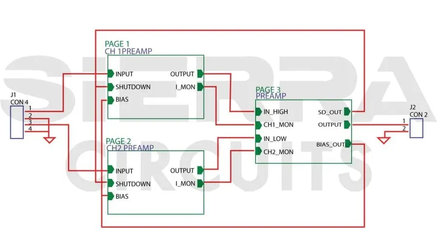
PCB Design Sketch
Before initiating a PCB design order, a thorough understanding of the project's requirements is paramount. This crucial initial step dictates the entire design process, encompassing not only the functional aspects of the circuit but also the physical constraints and material properties necessary for its intended application. A well-defined set of requirements minimizes costly revisions and ensures the final PCB meets all performance criteria.
Circuit Requirements This involves a comprehensive understanding of the electrical specifications, including voltage levels, current requirements, signal frequencies, impedance matching, and any specific analog or digital functionalities. Accurate determination of these parameters is essential for selecting suitable components and ensuring proper circuit operation.
Size Limitations Physical dimensions of the PCB are often constrained by the enclosure or system it will be integrated into. Therefore, the maximum allowable length, width, and height, including the thickness of the board and components, need to be specified to guide the PCB layout process. Size limitations can also impact component selection and routing complexity.
Material Specifications The choice of PCB material significantly impacts performance, reliability, and cost. Considerations include the dielectric constant, loss tangent, thermal conductivity, glass transition temperature (Tg), and coefficient of thermal expansion (CTE). The appropriate material should be chosen based on factors like operating frequency, temperature range, and mechanical stresses. For example, high-frequency applications often require materials with low dielectric loss, while high-power applications may need materials with high thermal conductivity.
Functionality A clear definition of the intended functionality is crucial. What specific tasks will this PCB accomplish? This involves understanding the inputs and outputs, data processing requirements, power consumption needs, and any communication interfaces. Knowing the intended use helps determine the necessary components, their arrangement, and the overall design approach. This also encompasses any unique features or performance requirements, such as high-speed data transmission, power management, or signal conditioning.
Selecting Your PCB Design Software
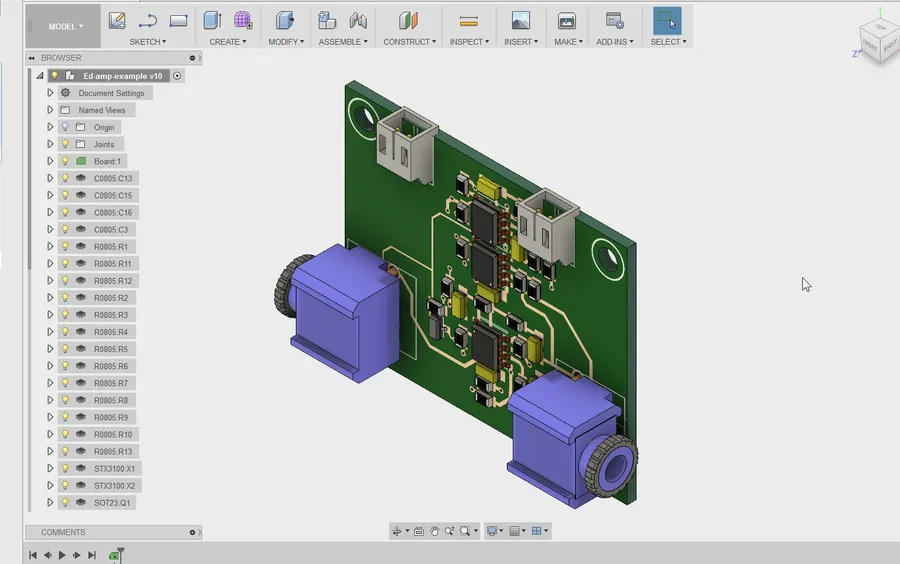
PCB Design Software Interface
The selection of appropriate PCB design software is a pivotal step in the PCB design order process, directly influencing design efficiency and accuracy. This choice ranges from cost-effective, entry-level options to advanced, comprehensive suites, aligning with project complexity and financial constraints. Key considerations include user interface intuitiveness, support for industry-standard file formats such as Gerber, and the availability of robust online support and community resources.
Feature
Basic Software
Advanced Software
Cost
Often free or low-cost
Subscription-based or expensive license
Ease of Use
User-friendly interface, suitable for beginners
Steeper learning curve, suitable for advanced users
Functionality
Limited to essential features
Comprehensive features including simulation, complex routing, and advanced analysis
File Format Support
Gerber, some other formats
Wide range of formats including STEP, IDF, and more
Support
Limited community or basic tutorials
Extensive online support, documentation, and training
Project Scope
Suitable for hobbyist and small projects
Suitable for complex projects and commercial use
Ease of Use A crucial factor, especially for beginners, is the software's user interface and overall intuitiveness. Software with a shallower learning curve ensures faster project initiation and fewer design errors during initial stages.
File Format Compatibility Compatibility with industry-standard file formats, such as Gerber, is essential for seamless integration with PCB fabrication services. Also, the compatibility with other file formats like STEP is necessary for complex designs that require 3D modelling and collaboration with other engineering tools.
Online Support Access to comprehensive online documentation, tutorials, and a responsive community can greatly aid in troubleshooting and optimizing design workflows.
Simulation Capabilities Advanced simulation tools help in validating designs and minimizing errors before manufacturing. This saves costs and improves the reliability of the PCB.
Component Libraries Availability of extensive and updated component libraries ensures that designers are using correct footprints and part parameters that are essential for a smooth and accurate PCB design process.
Schematic Capture and PCB Layout
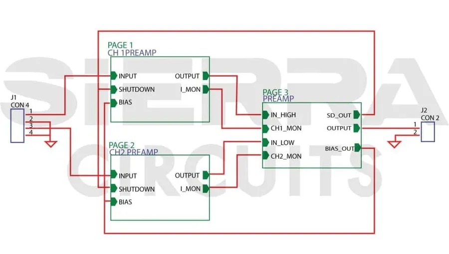
PCB Schematic Diagram
Schematic capture and PCB layout are pivotal stages in the PCB design process. Schematic capture involves creating a digital representation of your electronic circuit, while PCB layout translates this schematic into a physical arrangement of components, traces, and pads. This phase is critical for ensuring that the final PCB functions as intended, meeting all electrical and mechanical specifications.
This process is not merely about drawing lines and placing components; it's a complex task that demands careful consideration of electrical properties, thermal management, and manufacturability. Accurate execution during this phase directly impacts the performance, reliability, and cost of the final product.
Component Selection and Footprints Choosing the right components involves not only their functional specifications, but also their physical size and footprint. A footprint is the physical pattern of pads on the PCB where the component leads are to be soldered. Accurate footprints are vital for assembly.
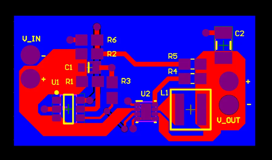
Optimal Component Placement Placing components logically and strategically is essential for minimizing signal interference, thermal issues, and manufacturing difficulties. Components should be arranged in a way that facilitates efficient signal flow and reduces the risk of shorts.
Trace Routing The routing process connects component pins using conductive paths (traces). This must be done while adhering to design rules like trace width, spacing, and impedance control. Improper trace routing can lead to signal integrity issues or reduced performance.
Design Rule Checking PCB layout must conform to design rules to ensure proper manufacturing. These include minimum trace width, minimum space between traces, and via size. Software tools can automate design rule checking (DRC), highlighting any violations, which must be corrected before proceeding to fabrication.
Consideration
Impact
Component Footprint Accuracy
Ensures proper solderability and reliable assembly. Inaccurate footprints can lead to component misfits.
Component Placement Strategy
Optimizes signal flow, reduces noise, and manages thermal dissipation. Poor placement can degrade performance.
Trace Width and Spacing
Determines current carrying capacity and prevents short circuits. Violations can result in overheating or circuit failure.
Layer Stack-up
Affects signal integrity, impedance control, and manufacturing cost. Poor layer selection can cause signal problems or increase production expenses.
Generating Gerber Files: Preparing for Fabrication
Gerber Files
The culmination of your PCB layout efforts is the generation of Gerber files, the standardized language understood by PCB manufacturers. These files precisely describe each layer of your board, ensuring accurate fabrication. Proper generation and verification of these files are critical to avoid costly errors in the final product.
Gerber files are essential for communicating the specifics of your PCB design to the manufacturing facility. They include data for copper layers, solder mask, silkscreen, and drill locations. Each layer is typically represented by a separate file, which allows the fabrication equipment to accurately interpret the design.
Essential Gerber File Types Understanding the various Gerber file types is essential. These commonly include: copper layers (GTL, GBL for top and bottom layers), solder mask (GTS, GBS), silkscreen (GTO, GBO), drill files (TXT or EXCELLON format), and a board outline file. Not all PCB manufacturers use the same abbreviations.
Verification of Gerber Files Before submitting your files to a manufacturer, use a Gerber viewer software to ensure they accurately represent your design. It's crucial to check for any unexpected anomalies, like missing features or incorrect layer alignment. These viewers can save significant time and expense by catching errors early.
Common Gerber File Generation Issues One common issue is incorrect file generation settings that may result in missing layers or misaligned features. Additionally, be certain that the selected output format matches the specification the PCB manufacture requires, and that the appropriate units and coordinate systems are used.
Tips for Accurate Gerber Files Use your PCB design software's Gerber export settings carefully, ensuring all layers are exported. Always check the generated output using a Gerber file viewer that is different from your design software to catch potential software specific issues.
Choosing a PCB Manufacturer: Comparing Options
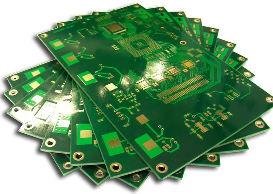
PCB Manufacturing Facility
Selecting the right PCB manufacturer is crucial for a successful project. The choice directly impacts the cost, turnaround time, and quality of your final product. This stage requires careful consideration of various factors, including the manufacturer's capabilities, pricing, and additional services offered.
Factor
Description
Considerations
Price
The cost per board and any additional fees.
Compare quotes for different quantities and specifications; look for hidden costs like tooling or expedited services.
Turnaround Time
The time from order placement to delivery.
Assess the manufacturer's standard lead time and understand options for rush orders, balancing the need for speed with costs.
Quality
The precision and reliability of the manufactured boards.
Check for certifications, customer reviews, and quality control processes; request samples or test boards when in doubt.
Materials
The types of materials that the manufacturer provides.
Ensure material is specified, FR-4, Rogers etc... and that they are suitable for your application
Additional Services
Options such as PCB assembly, stencil services, or DFM (Design for Manufacturability) checks.
Determine if you require these services and if the manufacturer offers them at a competitive price.
Capabilities
The technology that a manufacturer uses to fabricate PCBs
Is the technology, minimum trace width and layer count requirements supported.
Minimum Order Quantities
How many PCBs are required in a single order
Consider whether your project requires smaller or larger batches and if the manufacturers MOQ suits this.
Several manufacturers offer online quoting and ordering, simplifying the process. Popular choices include PCBWay, JLCPCB and DigiKey each with its unique strengths and specializations. PCBWay is known for its wide array of manufacturing options, JLCPCB offers competitive pricing for smaller runs, and DigiKey has a strong reputation for component distribution, and in addition, its PCB service is a growing option.
PCB Quote and Ordering Process: Step-by-Step
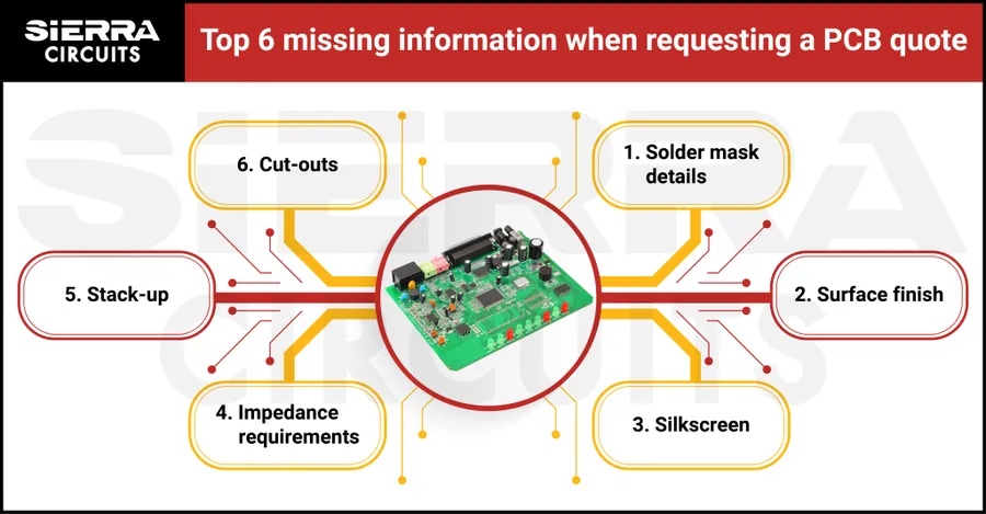
PCB Quote Sheet
The PCB ordering process is a critical step in bringing your electronic designs to life. It involves several key stages, from uploading your design files to receiving your finished boards. This section provides a step-by-step guide to navigate this process effectively, ensuring a smooth transition from design to physical product.
Prepare Your Gerber Files Ensure all necessary Gerber files for each layer of your PCB are generated correctly. This includes copper layers, solder mask, silkscreen, and drill files. Verify these files using a Gerber viewer to ensure accuracy before uploading.
Access the Manufacturer's Platform Navigate to the website of your chosen PCB manufacturer (e.g., JLCPCB, PCBWay, DigiKey). Most manufacturers have dedicated order pages or portals designed for this purpose.
Upload Gerber Files Use the manufacturer's provided tools to upload all your Gerber files. You might need to zip all the files into an archive before uploading. This might include the drill file and the netlist depending on the manufacturer.
Specify PCB Parameters You will need to specify several key parameters of your PCB. These generally include material type (e.g., FR-4), the number of layers, board dimensions (length, width and thickness), the desired copper weight, the colour of the soldermask, silkscreen, quantities required, surface finish, and any other specific requirements such as panelization or specific impedances. Accuracy here is key.
Review and Finalize Quote Once all the parameters are inputted, the manufacturer's system will generate a quote. Review all costs including material costs, any tooling and shipping, for accuracy and accept if everything is correct.
Payment Processing Once the quote has been accepted the payment process can begin. Follow the manufacturers guidelines to complete payment. This is usually via credit card, or some other online payment system, such as PayPal.
Production Commences Upon successful payment the manufacturer will then start production of your PCBs. At this point any issues with your designs or order specifications may result in delays or production holds.
Track Production and Delivery Most manufacturers provide order tracking through their online platform, enabling you to monitor the production and shipping status. You can use this tracking to estimate the delivery time to your location.
Tracking Your Order: Production and Delivery
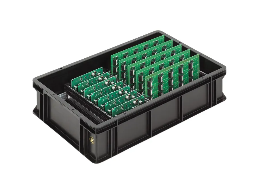
PCB Shipping
Following the placement of your PCB design order, a crucial phase begins: tracking production and delivery. Most PCB manufacturers provide robust tracking systems, allowing you to monitor your order's progression from fabrication to shipment. Understanding this process is essential for anticipating delivery timelines and managing your project schedule effectively.
Order Confirmation and Initial Status Immediately after placing your order, you should receive confirmation and an initial order status. This typically includes an order ID and a projected timeframe.
Fabrication Progress Tracking Most manufacturers provide updates on the fabrication progress, such as the start of production, the completion of each layer, and quality assurance checks. This stage is crucial for ensuring that your PCBs are manufactured correctly.
Shipping Updates and Tracking Numbers Once the PCBs are completed, the manufacturer will prepare them for shipping. You should receive shipping updates and tracking information from the courier service. The information provided will allow you to track the package while it is in transit.
Estimated Delivery Times and Considerations Delivery times vary depending on your location and the selected shipping method, usually from a few days to a couple of weeks. You should factor in potential delays during holidays and customs clearance if required. If you have specific delivery timeline requirements, discuss them with the manufacturer before ordering.
Communication with the Manufacturer Should you encounter any issues during the tracking process or experience unexpected delays, it's important to communicate with your manufacturer directly for updates and support.
Quality Control and Assembly
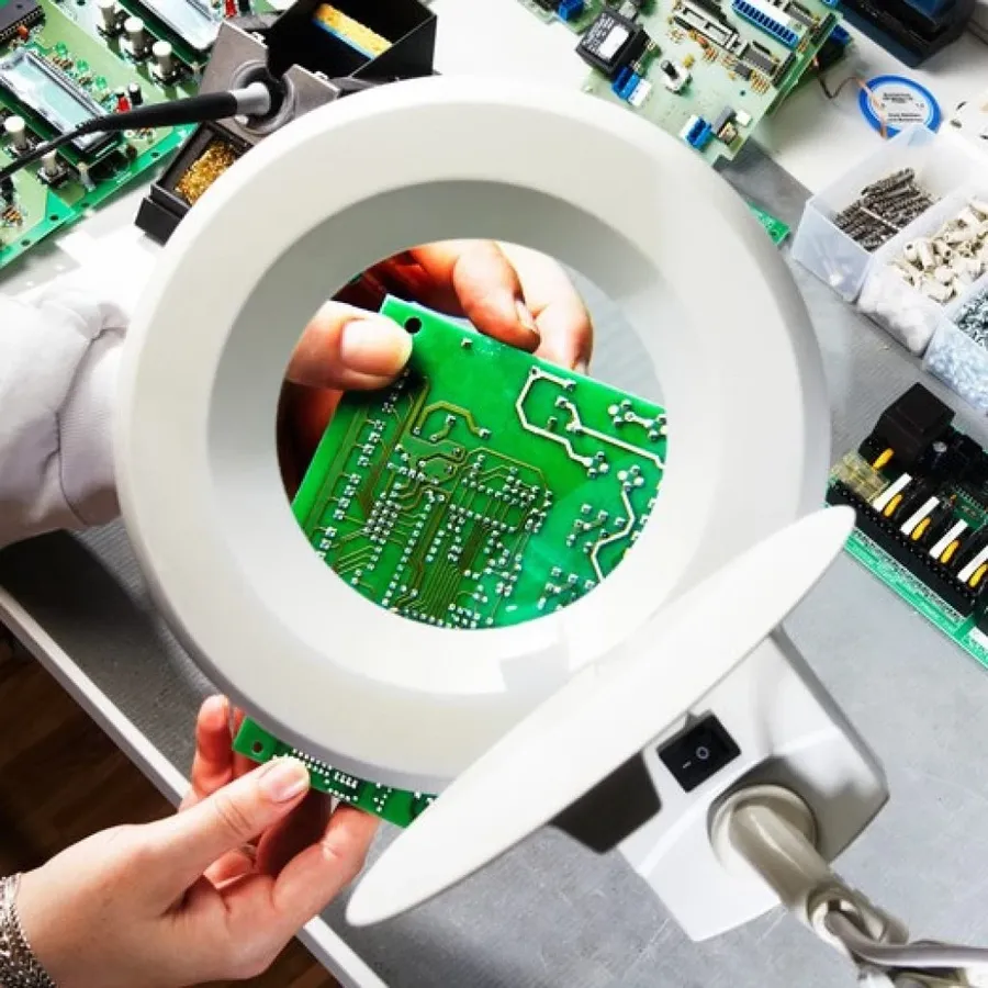
PCB Quality Inspection
Rigorous quality control upon arrival of your PCBs and meticulous component assembly are crucial final steps in ensuring a functional and reliable finished product. This stage validates the manufacturing process and transforms the bare PCB into a fully operational electronic device.
Visual Inspection Thoroughly examine the delivered PCBs for any physical defects such as scratches, breaks, misaligned layers, or inconsistencies in the solder mask or silkscreen. Pay close attention to fine-pitch components and trace widths.
Dimensional Verification Use calipers or a precision ruler to verify that the board dimensions match your design specifications. Confirm the accuracy of hole sizes and component pad locations.
Electrical Testing (Optional) For more complex designs or critical applications, an electrical test such as a 'flying probe test' or a bed of nails test can verify the integrity of the PCB's connectivity. This step can reveal shorts, opens or impedance issues.
Component Placement Use your Bill of Materials (BOM) to ensure you have all the necessary components. Start placing components according to your layout, starting with the most difficult to mount components first.
Soldering Apply the appropriate soldering technique, whether it be reflow soldering for surface mount components or through-hole soldering for traditional components. Ensure consistent and complete solder joints and avoid bridging between pads.
Post Assembly Inspection After soldering, perform another detailed inspection to identify any potential solder defects like cold solder joints or solder bridges. Use magnification if needed. Consider X-ray inspection for hidden solder joints if available.
Functional Testing Finally, perform functional tests based on the design requirements. Power up the board, perform software tests, and measure critical voltage and current levels, to confirm the PCB is operating as intended.
Frequently Asked Questions About PCB Design Orders
Navigating the PCB design and ordering process can be complex. This section addresses common questions to provide clarity and ensure a smoother experience.
What are the different types of PCB materials, and which is best for my project? PCB materials vary in their dielectric constant, thermal properties, and cost. Common materials include FR-4, which is versatile and cost-effective, and materials like Rogers which exhibit higher performance at radio frequencies. The ideal choice depends on your application's specific requirements, such as operating frequency, temperature range, and mechanical stress.
How do I determine the correct layer stackup for my PCB? The layer stackup refers to the arrangement of copper and dielectric layers in your PCB. Selecting the correct stackup is crucial for impedance control, signal integrity, and electromagnetic compatibility. The stackup will be determined by the complexity of your circuit, the signal types, and the required impedance characteristics. It is recommended to consult a stackup design tool from PCB manufacturers and industry guidelines to ensure proper performance.
What does 'Through-Hole' and 'Surface Mount' mean, and which should I use? Through-Hole (TH) refers to components with leads that pass through holes in the PCB and are soldered on the opposite side. Surface Mount (SMT) components are soldered directly to the surface of the PCB using pads on the surface. SMT allows for higher component density and automation, and is the common choice for most modern PCBs. Through-hole technology is often used for larger, robust components or when mechanical stress is high.
Can I test my PCB design before manufacturing? Yes, simulation and testing are critical before manufacturing. You should verify your schematic, check the design rules in your PCB software, and simulate signal integrity. Consider also a prototype order, before placing a larger order. This will allow you to identify and correct any issues before committing to full-scale production.
How do I generate Gerber files for my PCB design? Gerber files are the standard format for PCB fabrication. Your PCB design software will have a 'generate gerber' or 'plot' function that creates these files. Ensure you select all layers (copper, silkscreen, solder mask, drill), then verify the generated files against your design specifications before submitting them for manufacturing.
What are the key factors to consider when choosing a PCB manufacturer? Key factors to consider when selecting a PCB manufacturer are production cost, lead time, quality, and support. Also ensure that your chosen manufacturer has experience with the specific type of PCB you are producing and will be able to meet any design specifications (layer counts, tight tolerances etc). It is worthwhile comparing quotes from several manufacturers to find the best fit.
The PCB design order process can seem daunting at first, but by breaking it down into these manageable steps, anyone can navigate from idea to physical product. Understanding the process ensures that your PCB design order flows smoothly from the initial design to final delivery. Always remember to do your research and compare vendors to get the best quality and best fit for your project and be sure to understand all the necessary PCB requirements before commencing your project, making sure everything is in place for a smooth and efficient PCB design order process.