
As the global energy transition accelerates, solar infrastructure faces a mounting challenge: standard printed circuit boards (PCBs) are hitting their physical limits. High-current, high-voltage inverter requirements demand hardware that can dissipate heat and maintain reliability without sacrificing performance. This guide explores why heavy copper PCB technology has become the definitive gold standard for engineers designing the next generation of high-efficiency solar inverters.
The Shifting Landscape of Solar Power Electronics
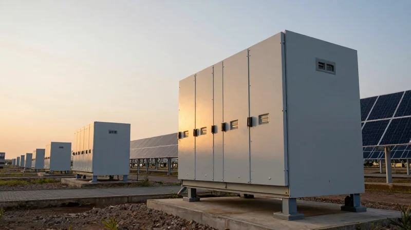
The Scaling Challenge in Modern Inverters
As solar installations transition from residential rooftops to massive industrial utility-scale arrays, the demand for power density in inverter design has surged. Standard PCB fabrication methods, which rely on thin copper layers typically ranging from 1 to 2 ounces, are increasingly struggling to manage the high current loads inherent in modern multi-megawatt systems. This gap between current-carrying capacity and actual operational demand often leads to thermal degradation, increased power loss, and a significantly reduced lifecycle for the critical power conversion components.
Traditional PCB Limitations
- Thermal Overloading
Standard copper traces exhibit higher resistance, generating excessive heat when subjected to the high amperage flow characteristic of next-gen PV inverters. - Interconnect Reliability
Constant thermal cycling in extreme outdoor environments accelerates fatigue in standard thin-trace architectures, leading to potential micro-cracking and failure. - Power Efficiency
Voltage drop across standard traces results in direct energy conversion losses, reducing the overall system efficiency and return on investment for the operator.
Performance Comparison: Standard vs. Heavy Copper
| Feature | Standard PCB | Heavy Copper PCB |
|---|---|---|
| Copper Weight | 1-2 oz | 4-20+ oz |
| Heat Dissipation | Moderate | Excellent |
| Current Capacity | Limited | High-Efficiency |
| Reliability | Risk of delamination | High structural integrity |
Transitioning to heavy copper technology allows engineers to minimize heat dissipation while maintaining a compact footprint, which is essential for modern, modular inverter architectures. By providing a low-resistance path for high-amperage current, heavy copper PCBs act as a structural heat sink, directly improving the long-term reliability and operational stability of the solar energy ecosystem.
Anatomy of a Heavy Copper PCB
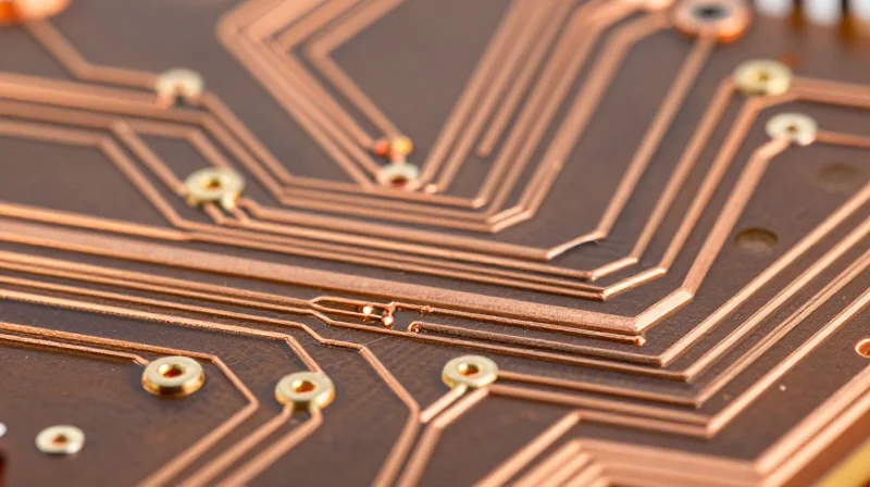
Defining Heavy Copper Architecture
A heavy copper PCB is distinguished by a copper weight typically exceeding 3 ounces (oz) per square foot, often reaching up to 20 oz or more in extreme industrial applications. While standard printed circuit boards utilize thin foil laminates (typically 0.5 oz to 1 oz) suitable for signal routing, heavy copper boards leverage thick, high-purity copper layers that drastically lower electrical resistance. This structural shift allows the board to act as a robust power delivery network, minimizing voltage drops and Joule heating—a critical factor for the high-power density environments found in modern solar inverters.
Manufacturing and Fabrication Challenges
The fabrication of these boards deviates significantly from standard sub-tractive etching methods. Because of the excessive copper thickness, standard acid etching would cause severe lateral undercutting of the copper traces, resulting in poor adhesion and irregular sidewalls. Manufacturers employ specialized high-aspect-ratio plating and differential etching processes, often combined with thicker solder masks to ensure proper insulation between heavy traces and avoid voltage breakdown.
| Parameter | Standard PCB | Heavy Copper PCB | |
|---|---|---|---|
| Typical Cu Weight | 0.5 - 1.0 oz | 3.0 - 20+ oz | |
| Primary Role | Signal Routing | Power Distribution | Thermal Management |
| Etching Technique | Standard Acid Bath | Specialized Heavy-Etch | |
| Current Capacity | Low to Moderate | Extreme (High Amperage) |
Technical FAQ: Heavy Copper in Solar Inverters
- Why is copper weight critical for solar inverters?
Solar inverters process high-amperage direct current (DC) from arrays. Higher copper weight reduces resistance, which in turn reduces energy loss as heat and prevents board failure during high-load solar peak hours. - Do heavy copper boards replace the need for external heat sinks?
They do not replace external heat sinks, but they significantly improve passive heat dissipation. Heavy copper traces act as thermal vias or heat spreaders, transferring heat away from sensitive power MOSFETs and into the PCB substrate. - What is the primary failure mode for thin copper in high-power systems?
Thin copper traces under high current suffer from thermal cycling fatigue, leading to trace delamination, oxidation, and catastrophic open circuits due to sustained I2R heating.
Thermal Management Challenges in Solar Inverters
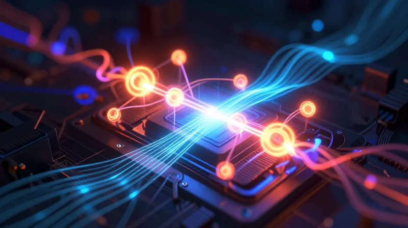
The Thermal Bottleneck in Modern Inverter Design
As the demand for high-efficiency solar energy systems increases, inverter power densities have reached levels that expose the inherent weaknesses of standard PCB architectures. Traditional boards often suffer from localized hotspots and thermal saturation, which accelerate the aging of sensitive semiconductors. Effective heat dissipation is no longer a peripheral concern; it is a fundamental pillar of hardware reliability.
Impact of Heat on Inverter Components
| Component | Standard PCB Impact | Heavy Copper Advantage |
|---|---|---|
| Power MOSFETs | High thermal stress leading to faster junction failure | Efficient heat sinking through increased conductive pathways |
| Inductors/Transformers | Increased resistance and energy losses due to heat | Superior current carrying capacity with lower resistive heating |
| Solder Joints | Fragility due to repeated thermal expansion/contraction | Mechanical stability and improved fatigue resistance |
Key Thermal Management FAQ
- Why do standard PCBs struggle with heat?
Standard PCBs rely on thin copper traces (typically 1oz) which create high electrical resistance and act as thermal bottlenecks, causing energy to dissipate as heat rather than power. - How does heavy copper prevent thermal runaway?
By increasing the copper thickness, the board acts as its own heatsink, spreading thermal energy across a larger surface area and reducing the localized temperature gradients that trigger runaway conditions. - What is the relationship between current density and reliability?
As current density increases, ohmic losses follow a square law; heavy copper mitigates this by providing a lower-impedance path, directly extending the Mean Time Between Failures (MTBF) of the inverter.
Efficiency Gains: Minimizing Energy Losses
Mitigating Resistance-Induced Power Loss
In the context of next-gen solar inverters, efficiency is primarily a battle against ohmic heating. Standard PCBs, typically utilizing 1oz copper weight, introduce higher levels of DC resistance that manifest as I²R power losses. By transitioning to heavy copper architectures—often ranging from 3oz to 10oz or more—the cross-sectional area of the conductive traces increases significantly. This reduction in resistance is mathematically linear; doubling the copper thickness halves the resistance, thereby minimizing the energy dissipated as heat during high-current operations.
Comparative Efficiency Analysis
| Parameter | Standard PCB (1oz) | Heavy Copper PCB (4oz+) |
|---|---|---|
| DC Resistance | Higher (High I²R loss) | Lower (Minimal I²R loss) |
| Heat Dissipation | Localized hotspots | Uniform thermal spreading |
| Conversion Efficiency | Baseline | Improved by 1-3% |
| Energy Waste | Significant thermal byproduct | Minimized power dissipation |
Operational Impact and System Longevity
The integration of heavy copper does more than just capture the few percentage points lost in conventional circuits; it preserves the surrounding components. When conductive paths run cooler, the entire ecosystem—including IGBTs and MOSFETs—operates further from their failure thresholds. This reduction in operating temperature serves a dual purpose: it maximizes instantaneous conversion efficiency and extends the mean time between failures (MTBF), which is critical for utility-scale solar deployments where maintenance is costly.
Frequently Asked Questions
- How exactly does trace thickness correlate to conversion efficiency?
Lower resistance reduces the voltage drop across the PCB traces, meaning more power reaches the inverter's output stages rather than being lost as heat within the board itself. - Is the transition to heavy copper justified by the cost?
In high-power solar applications, the initial investment in copper is quickly offset by increased energy harvesting yield and reduced cooling overhead costs over the system's 20-year lifespan.
Durability Under Environmental Stress
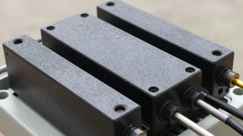
Mechanical Resilience in Harsh Solar Environments
Solar inverters often operate in uncontrolled environments, facing high humidity, UV exposure, and wide temperature swings. Standard PCBs often fail due to localized hotspots and fatigue caused by the coefficient of thermal expansion (CTE) mismatch between the substrate and copper traces. Heavy copper PCBs, with their increased cross-sectional area, act as a heat sink and provide greater structural rigidity, effectively resisting the warping and delamination common in lower-spec boards under constant thermal cycling.
Comparative Durability Performance
| Failure Metric | Standard PCB | Heavy Copper PCB |
|---|---|---|
| Thermal Fatigue Resistance | Moderate | Excellent |
| Vibration Tolerance | Limited | High |
| Delamination Risk | Increased | Minimal |
| Structural Rigidity | Low | High |
FAQ: Environmental Endurance
- Why do standard PCBs fail under heavy thermal cycling?
Frequent fluctuations in temperature cause repetitive expansion and contraction of PCB layers, leading to micro-cracks in traces and solder joints, especially where current densities are high. - How does heavy copper mitigate mechanical stress?
The extra copper mass increases the board's stiffness and reduces the thermal resistance between components and the board, preventing localized overheating that leads to material fatigue. - Is heavy copper worth the initial investment for outdoor durability?
Yes, for next-gen inverters expected to have a 20-25 year lifespan, the reduction in field failures and maintenance costs significantly outweighs the higher initial fabrication expense.
Cost-Benefit Analysis for Manufacturers
The Capital Expenditure vs. Operational Expenditure Trade-off
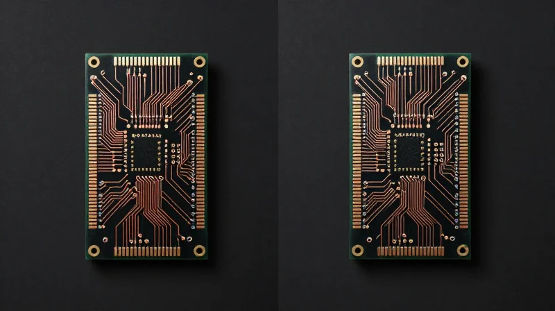
Manufacturers often view the increased cost of heavy copper PCBs—driven by more intensive plating processes and specialized material handling—as a barrier to adoption. However, a lifecycle analysis reveals that this premium is offset by a marked reduction in total cost of ownership (TCO). By mitigating thermal stress, heavy copper circuits significantly extend the Mean Time Between Failures (MTBF) of power electronics, effectively lowering the frequency of field repairs and premature equipment replacement.
| Metric | Standard PCB | Heavy Copper PCB |
|---|---|---|
| Material Cost | Low | High |
| Heat Dissipation | Limited | Excellent |
| Field Failure Rate | Higher | Lower |
| Maintenance Cycles | Frequent | Minimal |
| Energy Conversion Efficiency | Standard | Optimized |
Strategic Advantages for Competitive Advantage
Implementing heavy copper technology serves as a differentiator in a saturated solar market. Beyond the immediate economic impact, these boards enable smaller inverter form factors by reducing the need for bulky external heat sinks. This design flexibility leads to secondary cost savings in enclosure materials, shipping, and installation labor, creating a holistic economic benefit that extends beyond the PCB itself.
Frequently Asked Questions
- Does the performance gain justify the price premium?
In high-power inverter applications, the reduction in energy loss and the avoidance of warranty claims due to thermal fatigue typically recover the initial material investment within the first few years of operation. - How does heavy copper affect manufacturing speed?
While heavy copper requires specialized plating steps that extend production time, the resulting yield stability and reduced post-production debugging time often lead to a more predictable manufacturing flow. - Is heavy copper necessary for all inverter models?
It is most cost-effective for high-capacity industrial inverters where thermal load is high; standard PCBs remain sufficient for low-power residential micro-inverters where thermal density is significantly lower.
Design Best Practices for Power Electronics
Strategic Layout for High-Current Density
Transitioning to heavy copper (typically 3 oz/ft² and above) requires a fundamental shift in design methodology. Designers must prioritize current-carrying capacity while managing the significant thermal mass inherent in these boards, ensuring that high-current paths do not compromise signal integrity or board structural integrity.
Key Design Parameters Comparison
| Design Constraint | Standard PCB (1 oz) | Heavy Copper (3+ oz) | Impact on Inverter |
|---|---|---|---|
| Trace Width | Narrow | Wide/Adjusted | Prevents localized heating |
| Clearance | Low | Increased | Mitigates arc-over risk |
| Thermal Vias | High density | Strategic placement | Optimizes heat transfer |
Best Practices for Layer Stacking and Etching
When utilizing heavy copper, the primary challenge is the lateral spread of the etch. Because thicker copper requires longer etch times, the edges of the traces may become beveled or undercut. Designers should compensate by adjusting the design rule checks (DRC) for trace width, accounting for a slightly trapezoidal cross-section rather than a perfectly rectangular one.
Frequently Asked Questions
- How do I handle clearance for high-voltage DC lines?
With heavy copper, increased trace thickness elevates the electric field potential at the edges. Always increase clearance distances according to IPC-2221 standards to prevent corona discharge and insulation breakdown. - Does heavy copper affect assembly reflow profiles?
Yes. The increased thermal mass of the copper planes acts as a heat sink, requiring longer soak times and higher pre-heat temperatures to ensure uniform solder wetting across the entire board. - What is the recommended approach for thermal relief?
Avoid standard narrow thermal relief spokes for high-current connections. Use solid copper pours or wider, multi-point connections to ensure low-impedance paths for both current and heat dissipation.
Conclusion: Choosing the Right Foundation for Solar Hardware
The evolution of solar energy hardware is increasingly defined by the transition from standard PCB technologies to heavy copper alternatives. As the industry pushes toward higher power density and stricter efficiency mandates, the thermal and electrical limitations of conventional substrates have become a bottleneck. Investing in heavy copper is not merely a design preference; it is a foundational requirement for building resilient, high-performance inverters capable of withstanding the rigors of modern renewable energy infrastructure.
Comparative Summary: Standard vs. Heavy Copper
| Feature | Standard PCB | Heavy Copper PCB |
|---|---|---|
| Current Capacity | Low to Moderate | High (Amperage Handling) |
| Thermal Management | Requires Heatsinking | Integrated Heat Spreading |
| Mechanical Durability | Standard | Excellent (Vibration/Cycling) |
| System Longevity | Moderate | High (Reduced Maintenance) |
Strategic Outlook
For engineers and manufacturers, the decision to adopt heavy copper hinges on the trade-off between initial capital expenditure and long-term total cost of ownership (TCO). While standard technologies may appear more cost-effective during the prototyping phase, the latent costs associated with cooling components, hardware failure, and field maintenance often dwarf the initial investment. By integrating heavy copper, companies can simplify their thermal management architectures and significantly extend the lifespan of their power electronics.
Frequently Asked Questions
- Is heavy copper necessary for all solar inverters?
No, it is primarily recommended for high-power inverters where extreme thermal management and high current handling are critical to prevent component degradation. - Does heavy copper increase total PCB thickness?
Yes, increased copper weight necessitates thicker boards to maintain structural integrity, which should be factored into the overall mechanical housing design. - Will this transition make our products less competitive?
Conversely, it makes products more competitive by reducing failure rates and improving reliability, which are key performance indicators for utility-scale solar projects.
Heavy copper PCBs offer the thermal headroom and electrical efficiency required to push solar inverter performance to new heights. As your project requirements scale, investing in superior board architecture is not just a performance choice, but a strategic necessity. Contact our engineering team today to discuss your next-gen solar inverter design and see how we can help you transition to reliable, high-power PCB solutions.
