In today's world, custom printed circuit boards (PCBs) are at the heart of countless technological innovations, from smartphones to complex industrial machinery. Understanding the price of custom PCBs is crucial whether you're a hobbyist designing a small personal project or a professional developing large-scale electronic products. This guide provides a clear, easy-to-understand breakdown of how custom PCB price is determined, what factors influence it, and how to get the most value for your money. This article will also cover the latest information on custom PCB price. We will compare quotes and find the best custom pcb price to ensure your projects are successful and within budget.
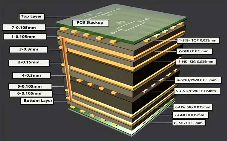
The cost of custom Printed Circuit Boards (PCBs) is not fixed; it's a dynamic value influenced by a multitude of factors. Understanding these elements is crucial for accurately estimating costs and optimizing designs for budget efficiency. Key determinants include the complexity of the design, material specifications, manufacturing processes, and order volumes. This section will delve into these individual factors to provide a comprehensive understanding of how they contribute to the overall price of a custom PCB.
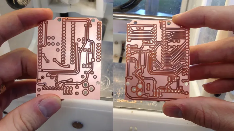
The number of layers in a Printed Circuit Board (PCB) is a primary determinant of its manufacturing cost, with the transition from single-layer to multi-layer designs resulting in a notable increase in expense. This escalation arises from the additional materials, processing steps, and precision required to fabricate boards with multiple conductive layers.
| PCB Layer Type | Complexity | Typical Applications | Cost Factor | Manufacturing Process |
|---|---|---|---|---|
| Single-Layer | Lowest | Simple circuits, basic electronics | Lowest | Simplest, one-sided etching |
| Double-Layer | Moderate | Intermediate circuits, dual-sided components | Moderate | Two-sided etching and plated through-holes |
| Multi-Layer (4+ Layers) | High | Complex electronics, high-density circuits | Highest | Lamination and multiple etching steps |
Multi-layer PCBs are indispensable for complex electronic designs due to their ability to accommodate denser circuitry, facilitate more intricate signal routing, and offer enhanced electromagnetic compatibility. The cost premium associated with multi-layer boards, however, necessitates careful evaluation during the design phase to ascertain the minimum number of layers needed to meet the specific functional requirements of the application. This approach ensures cost optimization without compromising design integrity.
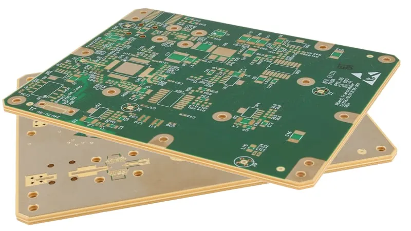
The selection of materials for a Printed Circuit Board (PCB) significantly impacts its cost, performance, and suitability for various applications. FR-4, polyimide, and other specialized materials each offer unique properties and price points, necessitating careful consideration during the design phase.
| Material | Description | Cost | Typical Applications |
|---|---|---|---|
| FR-4 | A glass-reinforced epoxy laminate, the most common PCB material. | Low to Moderate | General electronics, consumer products, most standard applications. |
| Polyimide | A high-performance polymer offering excellent thermal and electrical properties. | High | Aerospace, automotive, high-temperature environments, flexible circuits. |
| CEM-1 | A composite material with a paper core and glass layers. Lower cost alternative to FR-4 | Low | Single sided PCBs, less demanding applications. |
| Aluminum | Metal core material for superior heat dissipation | Moderate to High | LED lighting, power electronics, applications with thermal concerns. |
| Rogers | High-frequency laminates with excellent electrical performance. | High | RF and microwave applications, high-speed digital circuits. |
FR-4 is the most widely used PCB material due to its balance of cost, durability, and electrical performance. However, it may not be suitable for high-temperature or high-frequency applications, where materials like polyimide or Rogers laminates are preferred. Polyimide offers superior thermal stability and flexibility, making it ideal for harsh environments, but comes at a higher cost. Aluminum PCBs offer good heat dissipation for high power applications. Selecting a material that matches both the application requirements and budget constraints is crucial for cost-effective PCB manufacturing. It's important to note that material selection is not isolated, but is linked to other parameters like layer count, which in turn impacts cost.
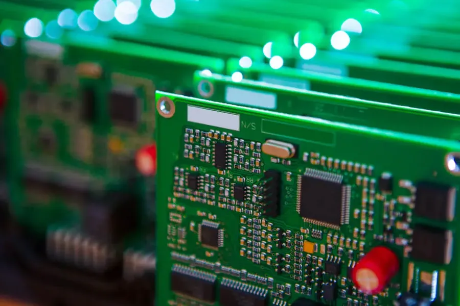
The physical size and dimensions of a Printed Circuit Board (PCB) are directly correlated with its manufacturing cost. Larger PCBs inherently require more raw materials, such as substrate and copper, leading to increased material costs. Additionally, the processing and handling of larger boards can also escalate expenses due to the necessity for larger equipment and more time-consuming processes.
Specifically, board size has a cascading effect on several aspects of PCB fabrication:
Given the direct relationship between board size and cost, minimizing board dimensions is essential for budget-conscious projects. Here's some practical advice for optimizing your board design:
Understanding and carefully managing PCB dimensions is crucial for managing costs effectively. A well-optimized layout not only reduces expenses but also ensures efficient resource usage during manufacturing.
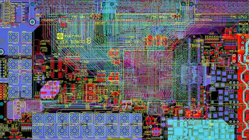
The intricacy of a PCB design directly impacts its manufacturing cost, with factors such as fine pitch components, via size, and trace width playing crucial roles. Complex designs necessitate advanced fabrication techniques, which increases the overall expense.
Understanding the cost drivers associated with design complexity can empower engineers to make informed decisions, balancing performance requirements with cost considerations.
| Design Feature | Impact on Cost | Optimization Strategy |
|---|---|---|
| Fine Pitch Components (e.g., BGA) | Increased cost due to higher precision required for placement and soldering. | Use components with larger pitch when feasible; consider design alternatives to reduce BGA usage. |
| Via Size (especially microvias) | Smaller vias increase drilling precision, leading to increased costs. Microvias require specialized processes. | Use larger vias where possible; minimize the use of microvias if cost is a concern. |
| Trace Width and Spacing | Narrower traces and tighter spacing need greater process control, raising the cost. | Design with wider traces and greater spacing where electrical requirements allow, reducing complexity. |
| Number of Solder Mask Layers | Increased number of solder mask layers and their complexity contribute to overall costs | Keep to the minimum number of layers required; simplify the design of the solder mask where feasible |
Optimizing PCB designs for cost-effectiveness involves a holistic approach that considers both functionality and manufacturability. By carefully evaluating the complexity of various design features, engineers can significantly reduce production expenses while maintaining the required performance standards. Collaboration with PCB manufacturers during the design phase is highly recommended, as they can offer valuable insights and suggestions to minimize production costs. For example, relaxing trace width and spacing requirements to the maximum allowable, while still meeting functionality criteria, can reduce costs.
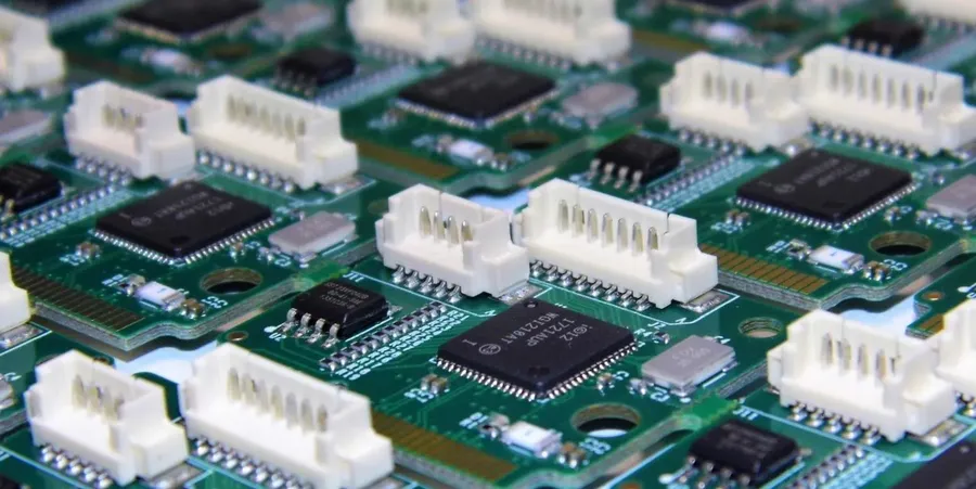
The unit cost of custom PCBs is significantly influenced by the order volume. As the quantity of PCBs increases, the cost per unit typically decreases due to economies of scale. This principle stems from the distribution of fixed costs, such as setup and tooling, across a larger number of units, leading to considerable savings for larger production runs.
| Order Volume | Cost per PCB | Total Cost | Cost Benefit |
|---|---|---|---|
| 1-10 | High | High | Low |
| 11-50 | Medium | Medium | Medium |
| 51-100 | Lower | Medium to High | High |
| 100+ | Lowest | High, but cost per piece is very low | Highest |
For small quantities (e.g., prototypes or initial tests), the per-unit cost can be substantial because a larger portion of the cost is attributed to setup and processing for a limited number of PCBs. However, when moving towards mass production, the savings per unit can be significant. Manufacturers often offer tiered pricing based on volume, with substantial discounts at higher quantities. This means that while the total cost of a large order will be higher, the price per PCB will be considerably lower.
Optimal order size depends heavily on project requirements, budget constraints, and future production needs. Consider factors like inventory capacity, storage solutions, and the potential need for reorders when making a decision. Accurate production planning to align with the expected need is vital to maximizing cost efficiency without holding unnecessary stock. Here are a few key considerations to help determine the optimal order size:
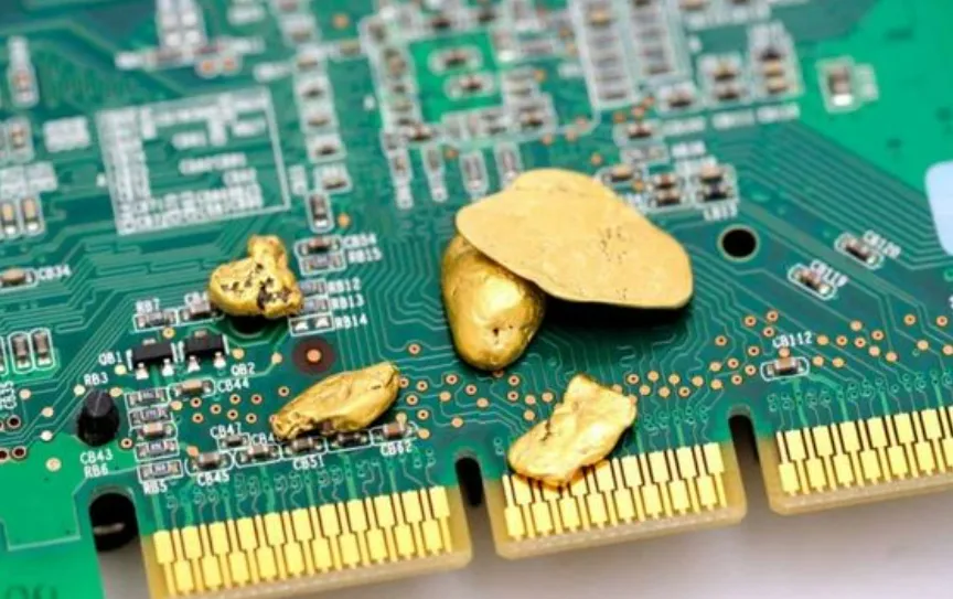
The surface finish of a printed circuit board (PCB) is a critical factor influencing its performance, durability, and ultimately, its cost. Different finishes offer varying levels of protection against corrosion and oxidation, impacting solderability and overall reliability. Selecting the appropriate finish is crucial to achieving desired functionality and cost targets.
| Surface Finish | Cost | Durability | Solderability | Typical Application |
|---|---|---|---|---|
| HASL (Hot Air Solder Leveling) | Low | Moderate | Good | General purpose, cost-sensitive applications |
| Lead-Free HASL | Low | Moderate | Good | RoHS compliant, general purpose |
| ENIG (Electroless Nickel Immersion Gold) | High | Excellent | Excellent | Fine pitch components, wire bonding, high reliability |
| OSP (Organic Solderability Preservative) | Low | Poor to Moderate (Short Shelf Life) | Good | Cost-sensitive, short-term storage and assembly |
| Immersion Silver (ImAg) | Moderate | Good | Excellent | Fine-pitch applications, good conductivity |
| Immersion Tin (ImSn) | Moderate | Moderate to Good | Good | Press-fit applications, good for signal transmission |
Each of these surface finishes provides a unique set of characteristics affecting cost, durability, and solderability. HASL is the most cost-effective but is less suitable for fine-pitch components, due to variations in surface thickness. ENIG, while more expensive, offers superior performance, is highly durable and delivers excellent solderability, making it the prefered choice for demanding applications. OSP, while low-cost, has a shorter shelf life and may not be ideal for products that require long storage before assembly. The choice of surface finish should always balance the requirements of the application with cost considerations.
Understanding the cost of custom PCBs can be complex, as multiple factors influence the final price. Below, we address some of the most common questions to help clarify this process.
Securing the best price for custom PCBs involves a strategic approach to comparing quotes from various manufacturers. This requires more than just looking at the bottom line; it involves a careful evaluation of several factors to ensure you're getting the best value, not just the lowest price. This section outlines critical aspects to consider when comparing quotes and choosing a suitable manufacturer.
Below are several aspects to consider when comparing quotes from different PCB manufacturers:
When choosing a manufacturer, focus on the overall value—the combination of cost, quality, and service—rather than just the lowest price point. While cost is a critical factor, it is crucial to ensure that you are not sacrificing quality or reliability.
| Factor | Importance | Description |
|---|---|---|
| Price | High | The total cost, including all associated fees. |
| Material Quality | High | The grade and certifications of materials used. |
| Manufacturing Capability | High | Ability to produce boards meeting your design requirements. |
| Customer Support | Medium | Quality and responsiveness of communication. |
| Lead Time | Medium | Time taken to produce and deliver the PCBs. |
| Production Capacity | Medium | The manufacturer's capability to handle your order volume. |
| Shipping Cost | Medium | Shipping cost and logistics efficiency. |
Reducing custom PCB costs requires a strategic approach that balances functionality with cost-effectiveness. By carefully considering design choices, material selections, and manufacturing processes, significant savings can be achieved without compromising the integrity of the final product. These strategies are critical for both prototype development and mass production.
Understanding the nuances of custom PCB price is crucial for managing project budgets effectively. By considering all the factors outlined – from layer counts and material choices to design complexity and production volumes – you can make informed decisions that lead to cost-effective PCB fabrication. Remember that a balance between cost and performance is key. Always aim to find the best value for your custom PCB needs by carefully comparing custom pcb price from multiple manufacturers. As technology evolves, so will the techniques for optimizing the cost and performance of custom PCBs, making continuous learning about new methods essential for successful project management.

