In today's world, printed circuit boards (PCBs) are the unsung heroes of nearly every electronic device, from smartphones to sophisticated industrial equipment. But what lies beneath the surface of these ubiquitous components? The answer is layers, each meticulously designed to fulfill specific functions. This article delves into the world of PCB layers, unraveling their structure, materials, and significance, and making the complex world of PCB design accessible and understandable.
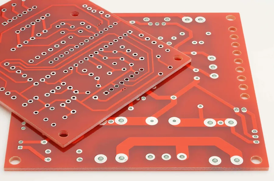
A PCB (Printed Circuit Board) layer is fundamentally a thin sheet of conductive material, most commonly copper, that is patterned to create conductive pathways, known as traces, for electrical signals and power. These conductive layers are meticulously etched and then laminated together with insulating dielectric materials to form the complete, functional circuit board. The strategic use of different layer types—signal, power, and ground—is critical for achieving desired electrical performance and functionality in electronic devices.
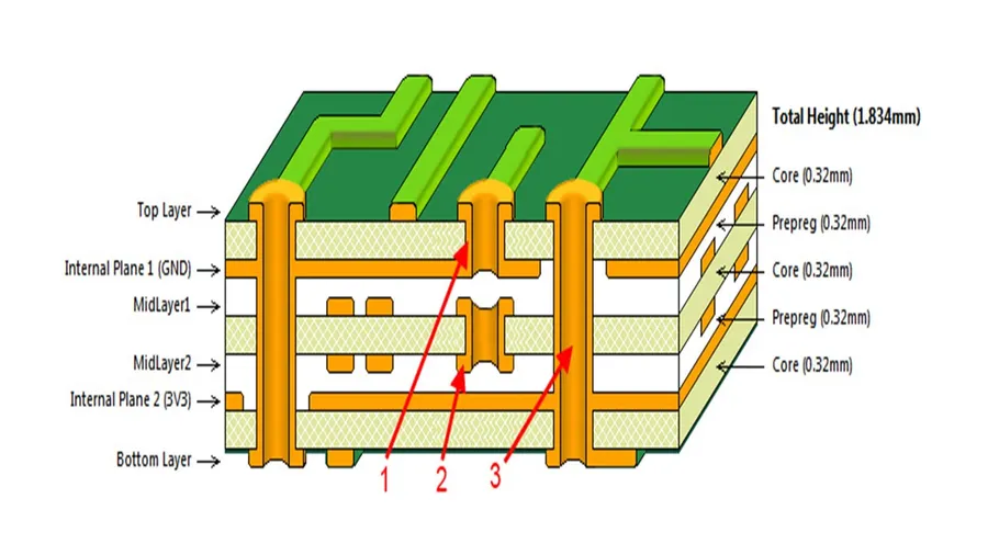
Printed circuit boards (PCBs) serve as the foundational platform for electronic circuits, with their design complexity scaling from single-layer to multi-layer configurations. The selection between these designs is dictated by the application's specific requirements, emphasizing trade-offs between simplicity and capability, and the fundamental role of the PCB layer.
| Feature | Single-Layer PCB | Multi-Layer PCB |
|---|---|---|
| Complexity | Simple design, one conductive layer | Complex design, multiple conductive layers |
| Cost | Lower production cost | Higher production cost |
| Density | Lower component density | Higher component density |
| Signal Routing | Limited routing options | Flexible routing options |
| Electromagnetic Interference (EMI) | Higher susceptibility to EMI | Lower susceptibility to EMI due to ground and power planes |
| Applications | Simple circuits, low-density devices | Complex circuits, high-density devices, high-speed applications |
| Layer Role | Single conductive layer for all signals, power, and ground. | Dedicated layers for signals, power, and ground, enhancing performance. |
Single-layer PCBs, with their straightforward construction featuring a single conductive layer, are suitable for basic electronic applications where circuit density and complexity are minimal. Their cost-effectiveness makes them attractive for simple projects. Conversely, multi-layer PCBs incorporate multiple conductive layers separated by insulating material. This structure facilitates complex routing and higher component density, while also improving electrical performance through dedicated power and ground planes. The strategic use of each PCB layer is central to optimizing overall board operation.
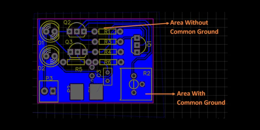
Printed circuit boards (PCBs) utilize a layered structure, with each layer serving a specific purpose in the overall functionality of the board. These layers are broadly categorized into signal layers, power planes, and ground planes, each contributing uniquely to the electrical performance of the PCB.
| Layer Type | Function | Characteristics | Best Practices |
|---|---|---|---|
| Signal Layers | Carry electrical signals for data transmission and control. | Traces are etched to create conductive pathways; various trace widths for different current and impedance requirements. | Minimize trace length, maintain consistent impedance, and avoid sharp bends to ensure signal integrity. |
| Power Planes | Distribute power at specific voltage levels to different components on the PCB. | Usually a large, solid copper area, often with multiple planes for different voltage rails; provides low impedance paths. | Use multiple power planes for different voltages; decoupling capacitors placed close to components; ensure proper thermal management. |
| Ground Planes | Provide a low impedance return path for signals and serve as a noise shield. | Usually a solid copper area; often connected to chassis ground for safety and EMI control; multiple ground planes can improve signal integrity. | Ensure good connections to ground pins and chassis; use multiple ground vias to minimize impedance. |
Signal layers are essential for routing traces that carry signals between different components. The careful design of signal layers, including trace width, spacing and layer assignment, is critical to ensure proper signal transmission without degradation. Power planes, often solid copper layers, act as reservoirs of electrical power, efficiently distributing voltage to various components. Proper use of these layers contributes to stable operation, minimizing voltage fluctuations. Ground planes offer a common reference point, providing a low-impedance return path for signals. This arrangement reduces noise and electromagnetic interference (EMI), greatly improving the signal integrity of the PCB. The arrangement of these layers in a PCB stack-up is also critical, and impacts the overall performance.
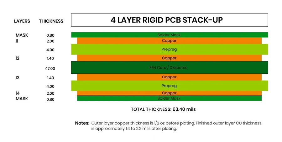
PCB stack-up refers to the arrangement and order of conductive and insulating layers within a printed circuit board. This configuration is crucial as it significantly impacts the board's electrical performance, signal integrity, and overall reliability. A well-planned stack-up ensures controlled impedance, minimizes signal reflections, and optimizes power distribution, while a poorly designed stack-up can lead to performance issues and board failures. Proper placement of each PCB layer is therefore essential for a functional and efficient circuit board.
| Factor | Impact | Mitigation |
|---|---|---|
| Impedance Control | Layer arrangement dictates the characteristic impedance of signal traces. | Carefully select layer spacing, dielectric materials and trace dimensions to achieve target impedance. |
| Signal Integrity | Layer stack-up affects signal reflections, crosstalk, and noise levels. | Strategically place ground and power planes to minimize noise and crosstalk; use proper trace routing. |
| Power Distribution | Power and ground plane placement affects voltage drop and noise. | Dedicate specific layers for power and ground; use decoupling capacitors close to active components. |
| Thermal Management | Layer stack-up can affect heat dissipation of components on the board. | Arrange the copper layers for proper heat transfer; implement thermal vias if required. |
| Manufacturing Cost | Layer count affects the cost of manufacturing of the PCB. | Choose the right number of layers based on complexity; consider cost-performance tradeoff. |
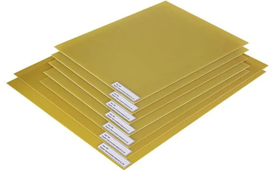
The performance and reliability of a Printed Circuit Board (PCB) are significantly influenced by the materials used in its construction, particularly within the layers. These materials can be broadly categorized into conductive materials, primarily copper, and dielectric materials, such as FR-4 and polyimide. The selection of these materials directly impacts the electrical, thermal, and mechanical properties of the final PCB.
| Material Type | Specific Material | Key Properties | Typical Applications |
|---|---|---|---|
| Conductive | Copper | High electrical conductivity, good thermal conductivity, easily etched | Signal layers, power planes, ground planes |
| Dielectric | FR-4 (Flame Retardant 4) | Good mechanical strength, cost-effective, moderate dielectric constant, flame retardant | General-purpose PCBs |
| Dielectric | Polyimide | High thermal stability, excellent electrical properties, flexible | High-temperature applications, flexible PCBs |
| Dielectric | Teflon (PTFE) | Low dielectric constant, low loss, high frequency performance | RF and high-speed digital PCBs |
| Dielectric | Ceramic | High thermal conductivity, high dielectric constant | High-power, high-frequency applications |
Copper, the primary conductive material, is chosen for its superior electrical conductivity, facilitating efficient signal and power transmission across the PCB. Dielectric materials serve as insulators between the conductive layers, preventing shorts and ensuring proper functionality. FR-4, a glass-reinforced epoxy laminate, is widely utilized due to its balance of performance and cost. For more demanding applications, polyimide offers enhanced thermal and electrical properties. Advanced materials such as PTFE and ceramic are also available for specific high performance applications.
The thickness of a PCB layer is a critical parameter impacting various aspects of circuit board performance. It directly influences trace impedance, current-carrying capacity, and thermal management, making it a fundamental design consideration. Selecting appropriate layer thicknesses ensures optimal electrical and thermal characteristics, while balancing cost and manufacturing feasibility.
| Parameter | Impact of Increased Thickness | Impact of Decreased Thickness |
|---|---|---|
| Trace Impedance | Decreases (for a given trace width) | Increases (for a given trace width) |
| Current Carrying Capacity | Increases | Decreases |
| Heat Dissipation | Improves | Worsens |
| Signal Integrity | Can improve in some cases by better control of impedance | May compromise if impedance not properly controlled |
| Manufacturing Cost | Generally increases, especially with thicker copper layers | Generally decreases, but may limit performance |
Standard copper foil thicknesses used in PCB fabrication are often measured in ounces per square foot (oz/ft²), which correlates to a specific thickness. Common thicknesses include 0.5 oz (approximately 0.7 mils or 18 microns), 1 oz (approximately 1.4 mils or 35 microns), and 2 oz (approximately 2.8 mils or 70 microns). Selecting the appropriate thickness requires careful analysis of both electrical and mechanical design specifications.
For signal layers, thinner copper is often used (e.g., 0.5 oz or 1 oz), balancing trace impedance requirements and cost. Power layers, designed to handle higher currents, typically utilize thicker copper (e.g., 1 oz or 2 oz). Dielectric layer thickness, commonly specified by the stack up design and impedance considerations, also plays a role, affecting the overall board thickness and electrical properties. Understanding these trade-offs is crucial for effective PCB design.
The number of layers in a PCB is not arbitrary; it's a critical design decision driven by several interconnected factors. These factors include circuit complexity, component density, signal speed, and cost considerations. Each additional PCB layer introduces increased design flexibility and performance capabilities but also contributes to higher manufacturing costs. Therefore, understanding these factors is paramount to achieving a balance between performance and cost-effectiveness.
| Factor | Description | Impact on Layer Count |
|---|---|---|
| Circuit Complexity | The intricacy of the circuitry and the number of independent signal paths. | More complex circuits with numerous signal paths generally require more layers to avoid signal crossing and ensure proper routing. |
| Component Density | The concentration of components on the board and the required space for interconnections. | High-density boards often need more layers for routing and efficient space management. Greater component density necessitates more layers to avoid overcrowding and ensure space for routing. |
| Signal Speed and Integrity | The operating frequencies of signals and the requirements for controlled impedance. | High-speed signals and the need for impedance control often require multiple signal layers and ground planes, increasing the total number of layers. |
| Power Distribution | The number of voltage rails needed to supply different components | Multiple power rails with high current demand might need dedicated power layers, adding to layer count |
| Budget Constraints | The overall cost limitations for manufacturing. | Adding more layers increases manufacturing costs. Balancing cost with performance is a key consideration. |
Each layer serves a specific purpose. Signal layers carry data and control signals, power layers distribute supply voltages, and ground layers provide a stable return path for currents and reduce noise. The arrangement and number of these layers are carefully considered during the stack-up design phase to optimize the PCB's electrical performance.
This section addresses common inquiries regarding PCB layers, providing clear and concise answers to enhance understanding of their structure and function. We'll delve into the reasons behind multi-layer PCB design choices, the significance of layer count, and the role of each layer.
Advanced PCB layer techniques are crucial for optimizing performance in high-speed digital and RF circuits. These techniques leverage innovative approaches to layer design and interconnections to improve signal integrity, reduce noise, and enhance overall circuit functionality. These techniques often involve precise control over layer characteristics and complex interconnection strategies.
Understanding PCB layers is fundamental for anyone involved in electronics design and manufacturing. From choosing the appropriate layer count to meticulous arrangement and material selection, every decision impacts the final product's functionality and reliability. As technology advances, the intricacies of [pcb layer] design will continue to play a vital role in driving innovation and creating cutting-edge electronic devices. Therefore, attention to detail on PCB layers is paramount for producing efficient, reliable, and high-performance electronics.

