The NPN transistor, a cornerstone of modern electronics, is a fascinating device that controls the flow of electrical current, much like a valve controls water flow. This fundamental component is present in countless devices, from everyday smartphones to advanced industrial systems. In essence, the NPN transistor is a type of bipolar junction transistor (BJT) built from three layers of semiconductor material, with an intriguing structure enabling amplification and switching of electrical signals. In this article, we will delve into the structure of the NPN transistor, understand its working principles, explore its diverse applications, and address common queries regarding its function, so get ready to explore the world of the ubiquitous and crucial NPN transistor!
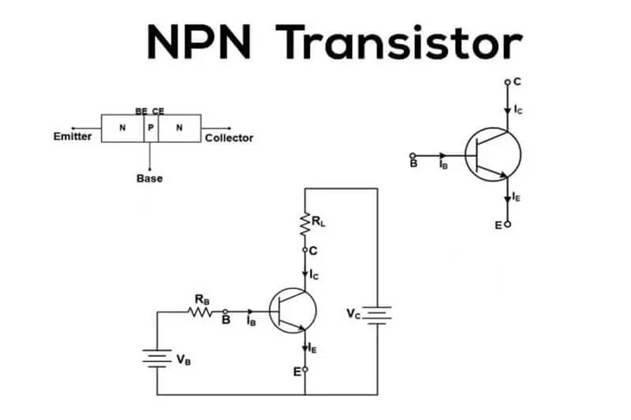
The NPN transistor, a cornerstone of modern electronics, is fundamentally constructed from three distinct layers of semiconductor material. Specifically, it comprises a P-type semiconductor layer positioned between two N-type semiconductor layers. This layered architecture, forming a 'sandwich' structure, is pivotal to the transistor's unique ability to control and amplify electrical signals. Understanding the properties and roles of each layer—the Emitter, Base, and Collector—is essential to grasping the operational principles of the NPN transistor.
| Layer | Type | Primary Function | Doping Level |
|---|---|---|---|
| Emitter | N-type | Supplies majority charge carriers (electrons) to the base. | Heavily doped |
| Base | P-type | Controls the flow of electrons from the emitter to the collector. | Lightly doped |
| Collector | N-type | Collects the electrons from the base. | Moderately doped |
The N-type semiconductor material is engineered to have an excess of free electrons, which act as majority charge carriers. Conversely, the P-type material is characterized by a deficiency of electrons, or holes, which act as majority charge carriers. This difference in doping characteristics enables the creation of PN junctions at the interfaces between the layers, which give rise to the unique behavior of the NPN transistor. The emitter is typically heavily doped to enhance its efficiency in injecting charge carriers into the base, while the base is lightly doped to minimize recombination of carriers and maximize current gain. The collector, although also N-type, is typically moderately doped.
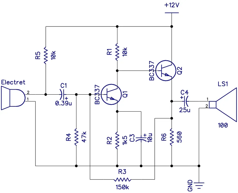
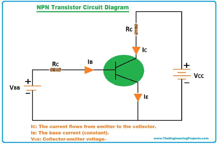
The NPN transistor's functionality hinges on its ability to control a large collector current with a much smaller base current. This control mechanism enables both amplification and switching applications. The core of its operation lies in the movement of electrons and holes within the semiconductor layers, which varies based on the applied bias voltages.
Fundamentally, the NPN transistor has three distinct operating regions: cutoff, active, and saturation. Each region dictates how the transistor responds to varying input currents and voltages, thereby establishing its usefulness in diverse electronic circuits. Understanding these regions is essential for effective application design.
The NPN transistor is represented by a specific schematic symbol that visually depicts its structure and electron flow, with each of its three pins—the emitter, base, and collector—having unique functions within the circuit, understanding this is fundamental to correctly integrating the NPN transistor into any electronic circuit.
| Component | Description | Symbol Representation |
|---|---|---|
| Emitter | The region that supplies charge carriers (electrons in NPN) to the transistor. This is typically shown with an arrow pointing away from the base. | Arrow pointing away from the base |
| Base | The control region of the transistor, a small current at the base controls the larger current flow between the emitter and collector. | Thin line connecting to the center. |
| Collector | The region that collects the charge carriers from the emitter. The collector often connects to the power supply in a common-emitter configuration. | Line connecting opposite to the emitter. |
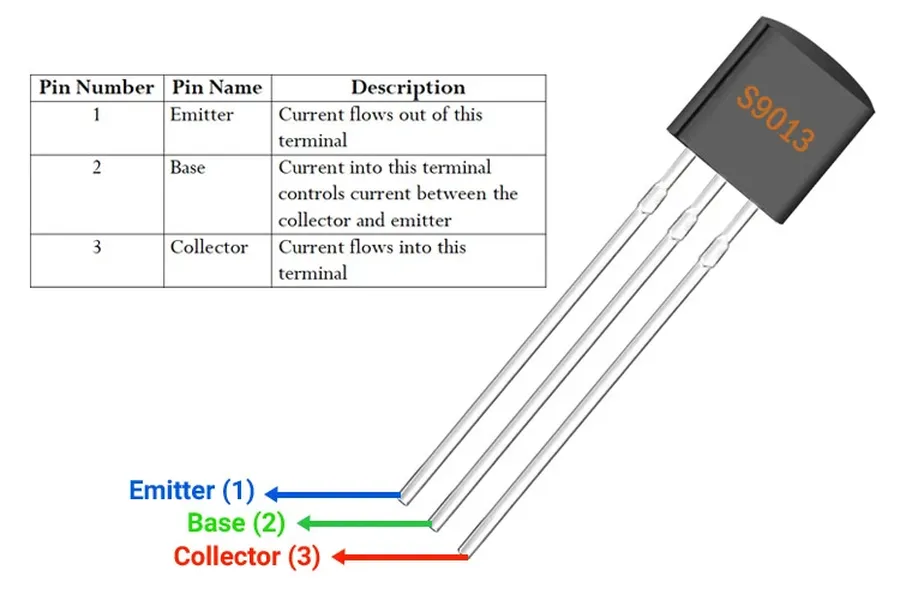
The pinout of an NPN transistor refers to the physical arrangement of the three leads, which are the emitter, base, and collector. The specific arrangement can vary based on the transistor package, which is typically documented in its datasheet, which is very important to reference when implementing any circuit.
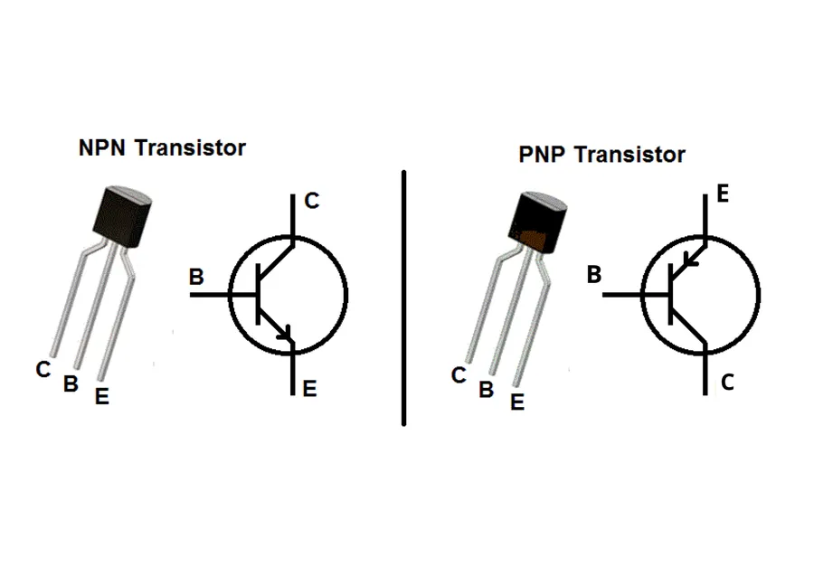
NPN and PNP transistors are bipolar junction transistors (BJTs) that serve as fundamental building blocks in electronic circuits, yet their operational characteristics and applications differ significantly due to the reversed polarities of their semiconductor layers. Understanding these distinctions is crucial for effective circuit design.
| Feature | NPN Transistor | PNP Transistor |
|---|---|---|
| Layer Configuration | N-type | P-type | N-type | P-type | N-type | P-type |
| Current Flow Direction (Conventional) | Collector to Emitter | Emitter to Collector |
| Biasing Voltage | Base positive relative to Emitter | Base negative relative to Emitter |
| Active Region | Positive Base Current enables Collector Current | Negative Base Current enables Collector Current |
| Majority Carriers | Electrons | Holes |
| On/Off Switching Logic | Active High (positive voltage at the base) | Active Low (negative voltage at the base) |
| Typical Use Cases | Low-side switching, signal amplification | High-side switching, power control |
The core difference lies in the arrangement of the semiconductor layers. NPN transistors consist of a P-type material sandwiched between two N-type materials, whereas PNP transistors have an N-type material between two P-type layers. This difference in structure dictates how current flows within each transistor type, consequently influencing their application in circuits. NPN transistors are typically employed in low-side switching and signal amplification, while PNP transistors are frequently used in high-side switching and power control applications.
When choosing between NPN and PNP transistors, consider the specific circuit requirements. If you need to switch a load connected to ground, an NPN transistor is often preferred. Alternatively, a PNP transistor is more appropriate for switching a load connected to the supply voltage. Understanding these subtle differences enables designers to utilize each transistor type effectively to achieve optimized circuit performance.
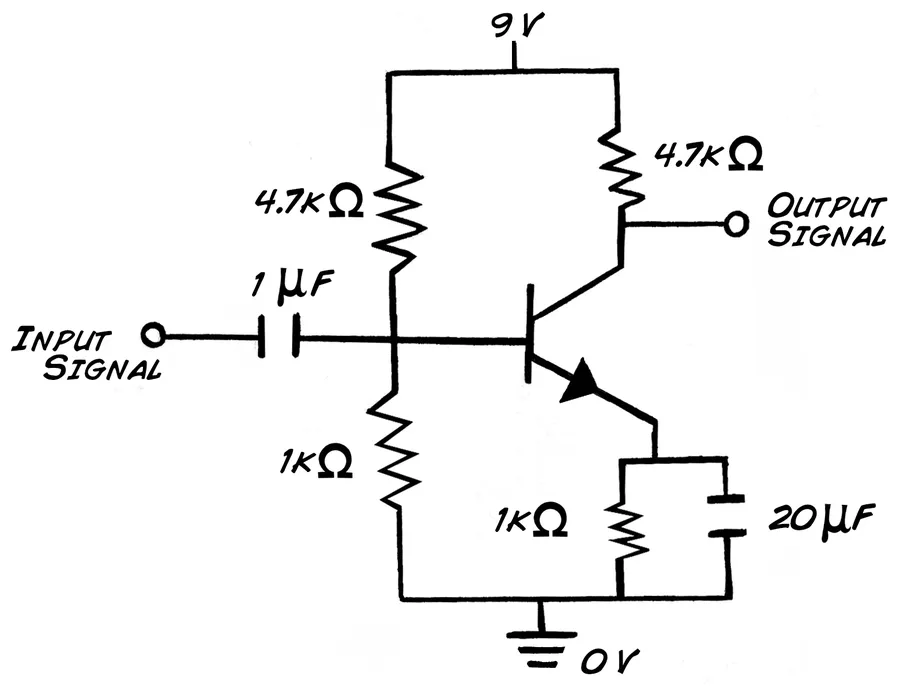
NPN transistors, due to their ability to amplify and switch electronic signals, are fundamental components in a wide array of electronic circuits. Their versatility stems from the precise control they offer over current flow, making them essential in numerous applications across various fields of electronics.
Below are some of the most common applications of NPN transistors:
Efficient testing and troubleshooting are critical for maintaining circuits employing NPN transistors. This involves using tools like multimeters to assess transistor health, identify common issues, and ensure reliable circuit operation. A systematic approach to testing can significantly reduce downtime and prevent costly failures.
Choosing the appropriate NPN transistor for a specific application is crucial for optimal circuit performance and reliability. This involves understanding key parameters detailed in datasheets and matching these specifications to the requirements of the circuit. Careful selection ensures the transistor operates within safe limits and achieves its intended function, whether it's amplification or switching.
| Parameter | Description | Importance |
|---|---|---|
| Current Gain (hFE) | The ratio of collector current (IC) to base current (IB). Often referred to as Beta (β). | Determines the transistor's amplification capability. A higher hFE indicates greater current gain. |
| Maximum Collector Current (ICmax) | The maximum allowable current that can flow through the collector without damaging the transistor. | Essential for preventing burnout; the circuit's current demand must be lower than ICmax. |
| Collector-Emitter Voltage (VCE) | The maximum voltage that can be applied between the collector and emitter terminals. | Important for ensuring the transistor operates safely and does not experience a voltage breakdown. |
| Maximum Power Dissipation (PDmax) | The maximum amount of power that the transistor can safely dissipate as heat. | Critical for thermal management; excessive heat can lead to transistor failure. |
| Transition Frequency (fT) | The frequency at which the transistor's current gain drops to unity. | Relevant for high-frequency applications; determines the useful frequency range of the transistor. |
| Operating Temperature Range | The range of temperatures within which the transistor operates reliably. | Important for applications where the transistor may be exposed to extreme temperatures. |
When selecting an NPN transistor, consider the following steps. First, assess the circuit requirements; determine the current, voltage, and frequency demands. Next, review manufacturer datasheets for various NPN transistors and compare them to circuit requirements. Finally, evaluate other factors like cost, availability, and form factor. If unsure, it is always best to select a transistor with specifications that exceed the application's requirements.
This section addresses common queries regarding NPN transistors, providing concise and authoritative answers to enhance your understanding of these fundamental semiconductor devices.
NPN transistor datasheets are crucial for selecting the correct component and designing reliable circuits. These documents provide essential information regarding the electrical characteristics and performance limits of the transistor. A thorough understanding of these parameters is vital for ensuring optimal circuit operation and avoiding damage to the device.
Key parameters found on NPN transistor datasheets include:
Understanding these key parameters allows engineers to make informed decisions when designing circuits with NPN transistors, ensuring the circuit performs as intended, safely and reliably.
The NPN transistor, a cornerstone in electronics, serves as a vital tool for both amplifying and switching signals. Its three-layer structure, involving two N-type regions sandwiching a P-type region, allows for precise control of electron flow. The NPN transistor is an essential component for modern technology, appearing in countless devices and systems, from simple circuits to complex machinery. By understanding its underlying principles, diverse applications, and the differences between NPN and PNP transistors, you can use NPN transistors effectively in electronic design and continue to push the boundaries of what is possible.

