In our increasingly interconnected world, the humble wiring board forms the backbone of countless electronic devices. From the simplest gadgets to complex industrial machinery, these boards provide the crucial pathways that allow electrical components to communicate and function. This article will delve into the intricacies of wiring boards, often referred to as printed wiring boards (PWBs), exploring their fundamental principles, diverse applications, and key differences compared to printed circuit boards (PCBs), thereby bridging the gap between user-level understanding and the underlying technology.
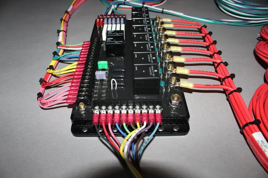
A Printed Wiring Board (PWB), often referred to as a bare board, serves as the foundational platform for electronic components in nearly all modern electronic devices. It provides both mechanical support and electrical pathways, allowing for the precise interconnection of these components to form functional circuits. This board is the critical base layer that, when populated with components, becomes a functional Printed Circuit Board (PCB).
The primary function of a PWB is to facilitate electrical conductivity between various components through etched conductive tracks. These tracks are made of copper, carefully routed to create the required electrical network. PWBs are typically manufactured using non-conductive substrate materials, such as FR-4 (Flame Retardant 4), which offer both mechanical strength and electrical insulation.
The construction of a PWB begins with a layer of insulating material that is then covered with copper foil. The copper is selectively etched to create the desired circuit pattern and then holes are drilled for component placement and interconnections. After this process the board is ready for the application of components. This process is crucial to electronics manufacturing as it ensures that components can be properly assembled and electrically connected.
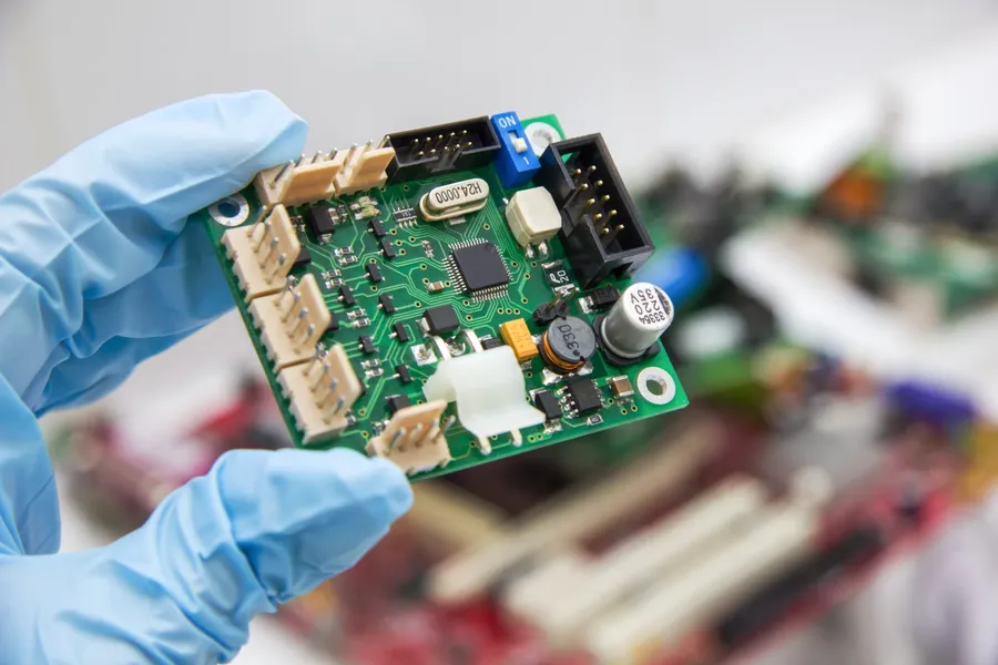
The terms Printed Wiring Board (PWB) and Printed Circuit Board (PCB) are often used interchangeably, but they represent distinct stages in the electronics manufacturing process. A PWB is the bare foundation, a substrate with conductive pathways, while a PCB is the fully functional board after electronic components have been mounted onto it. Understanding this distinction is critical for anyone involved in electronics design, manufacturing, or repair.
| Feature | Printed Wiring Board (PWB) | Printed Circuit Board (PCB) |
|---|---|---|
| Definition | Bare board with conductive tracks, pads, and vias. | PWB with electronic components attached. |
| Components | No components attached; only conductive pathways. | Components such as resistors, capacitors, ICs, etc., are soldered onto the board. |
| Function | Provides a mechanical and electrical foundation for component placement. | A fully functional electronic circuit. |
| Historical Context | The term 'PWB' is older, reflecting the earlier focus on point-to-point wiring. | The term 'PCB' emerged as component mounting became more integrated, and surface mount technology became commonplace. |
| Manufacturing Stage | An intermediate product in the board manufacturing process. | A finished electronic assembly. |
| Use Case | Used for mounting and connecting electronic components. | Ready for installation into electronic devices. |
The transition from PWB to PCB involves a critical stage of assembly where electronic components are placed and soldered onto the bare board. This transformation turns the PWB into a functional PCB, ready to be integrated into a final product. The design of both the PWB and the PCB is crucial for performance, reliability, and longevity of the resulting electronics assembly.
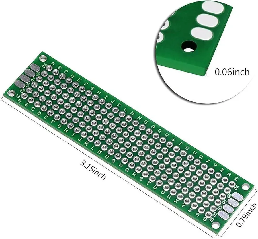
Wiring boards, the foundational structures for electronic circuits, come in various forms, each designed to meet specific application needs. The type of board used greatly impacts the performance, cost, and complexity of the final electronic product. These boards are classified based on the number of conductive layers and the materials used.
| Type of Wiring Board | Description | Common Materials | Advantages | Disadvantages | Typical Applications |
|---|---|---|---|---|---|
| Single-Sided Boards | Have conductive material (usually copper) on only one side of the board. | FR-4, CEM-1 | Low cost, simple design, easy to manufacture. | Limited component density, suitable for basic circuitry. | Simple consumer electronics, LED lighting, low-power devices. |
| Double-Sided Boards | Have conductive material on both sides of the board, allowing for more complex circuits. | FR-4, CEM-3 | Increased component density, more complex circuits, through-hole plating allows connections between sides. | Higher cost than single-sided boards. | Power supplies, audio equipment, more advanced consumer electronics. |
| Multi-Layer Boards | Consist of three or more layers of conductive material, separated by insulating layers. | FR-4, Polyimide | High component density, complex routing, excellent performance, compact design. | Highest cost, complex manufacturing processes, requires precise fabrication. | High-end computing, smartphones, aerospace, medical equipment. |
| Flexible Boards (Flex PCBs) | Use flexible substrates allowing for bending and shaping of the board. | Polyimide, Polyester | Flexibility, allows for integration in tight spaces, durable for dynamic applications. | Higher cost than rigid boards, less support for heavy components. | Wearables, cameras, automotive, space-constrained electronics. |
| Rigid-Flex Boards | Combination of rigid and flexible sections in the same board, offering both stability and flexibility. | FR-4 and Polyimide combination | Combines benefits of rigid and flex boards, versatile for complex designs. | Highest cost and design complexity. | Advanced medical devices, aerospace electronics, specialized robotics. |
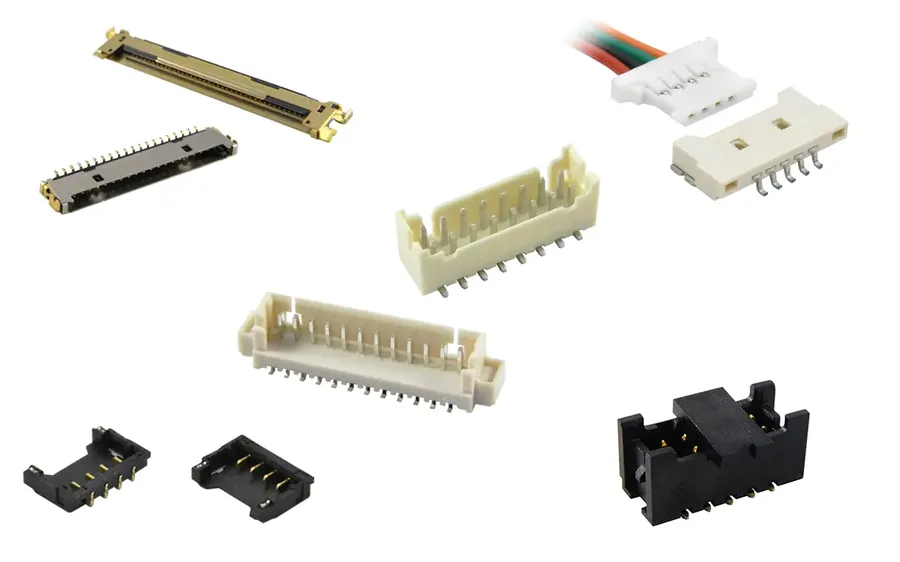
Wiring boards serve as the foundational platforms for electronic circuits, and their functionality relies heavily on the components mounted upon them. These components, including relays, fuses, connectors, and switches, are the building blocks of electronic systems, each playing a crucial role in the overall operation of the device.
Understanding the function of each component provides insight into how a wiring board facilitates the flow of electricity and information within a circuit. This section will explore common components, their functions, and how they integrate into overall device operation, providing specific examples such as the 3PDT wiring boards found in guitar pedals.
| Component | Function | Typical Application |
|---|---|---|
| Relays | Electrically operated switches that can control high-power circuits using a low-power signal. | Switching power circuits, motor control, automotive systems. |
| Fuses | Safety devices that protect circuits from overcurrent by breaking the circuit when a specific current threshold is exceeded. | Overcurrent protection in all electronic devices. |
| Connectors | Provide separable electrical connections between different parts of a circuit or between the board and external devices. | Data transmission, power input/output, signal routing. |
| Switches | Manually or automatically control the flow of current in a circuit, enabling or disabling specific functions. | User interface for devices, control circuits, signal selection. |
| 3PDT Switches | A specific type of switch with three poles and two throws, commonly used for complex switching patterns. | Bypass circuitry and complex signal routing in guitar effects pedals. |

Effective wiring board design is crucial for ensuring optimal performance and reliability of electronic devices. It involves a careful consideration of various factors, from physical layout to material selection, all of which influence signal integrity, thermal management, and the overall functionality of the final product. A well-designed board minimizes signal interference, manages heat effectively, and facilitates efficient manufacturing and assembly processes.
| Design Factor | Description | Impact |
|---|---|---|
| Layout | The physical arrangement of components and traces on the board. | Determines signal path lengths, reduces crosstalk, and facilitates efficient heat dissipation. Poor layout can lead to signal integrity issues, overheating, and increased manufacturing complexity. |
| Trace Width and Spacing | Dimensions of conductive paths and the gaps between them. | Affects current carrying capacity, impedance, and signal integrity. Insufficient width leads to higher resistance, voltage drop, and thermal issues. Inadequate spacing leads to shorts and crosstalk. |
| Component Placement | Location and orientation of electronic components on the board. | Influences signal paths, thermal management, and assembly. Poor placement can lead to signal integrity issues, difficulty in assembly, and ineffective heat dissipation. |
| Material Selection | Choice of materials for the board substrate and conductive layers. | Affects electrical and mechanical properties, as well as cost. FR-4 is common for rigid boards; flexible substrates for flexible applications. Material choice impacts thermal management, signal integrity, and reliability. |
| Design Rules and Best Practices | Industry standards and established guidelines for board design. | Ensure manufacturability, reliability, and performance. These practices minimize risks such as signal reflections, interference, and manufacturing defects. |
| Signal Integrity | Maintaining signal quality during transmission. | Critical for high-speed applications. Proper trace impedance matching, shielding, and minimizing discontinuities are vital. |
| Thermal Management | Effective dissipation of heat generated by components. | Prevents overheating and ensures long-term reliability. Thermal vias, heat sinks, and strategic component placement help manage heat. |
| Reliability | Ensuring long-term stable operation of the board. | Achieved through adherence to good design practices, component selection, and thorough testing. |
The manufacturing of wiring boards, a crucial step in electronics production, involves a series of precise processes that transform design specifications into a physical product. These processes encompass various techniques such as etching, drilling, plating, and quality control, all of which contribute to the functionality and reliability of the final electronic device.
| Process | Description | Equipment |
|---|---|---|
| Imaging | Transfer circuit design to board | UV Light Source, Photomask |
| Etching | Remove unwanted copper | Chemical etchants, Etching machine |
| Drilling | Create component mounting holes | CNC drilling machines |
| Plating | Deposit conductive layers | Electrolytic plating baths |
| Solder Mask | Apply protective layer to board | Screen Printing Machine |
| Silkscreen Printing | Add informative markings | Silkscreen Machine |
| Inspection and Testing | Ensure board quality | Automated Optical Inspection (AOI) |
The cost-effectiveness of wiring board manufacturing is heavily influenced by factors such as material selection, the complexity of the design, and production volume. High-quality manufacturing processes are paramount to ensure the reliability and optimal performance of the boards within electronic devices.
Effective troubleshooting of wiring board issues is crucial for maintaining the functionality and reliability of electronic devices. This section addresses common problems like shorts, open circuits, and component failures, offering practical diagnostic and repair strategies.
In addition to the above, it is also important to consider the following points during troubleshooting:
This section addresses common inquiries about wiring boards, providing clear and concise explanations to enhance understanding and resolve user concerns. These FAQs aim to clarify fundamental concepts, practical applications, and differences between similar terms in the electronics field.
The future of wiring board technology is poised for significant advancements, driven by the demand for more compact, flexible, and high-performance electronic devices. Key trends include the adoption of flexible materials, the push towards miniaturization, and the integration of artificial intelligence in design and manufacturing processes. These advancements are expected to revolutionize the functionality and application of electronic products across various industries.
Wiring boards, the unsung heroes of modern electronics, are the critical platform on which components are mounted and interconnected to facilitate functionality. Understanding the nuances between PWBs and PCBs, the various design considerations, and practical knowledge related to their manufacture and troubleshooting is crucial. Whether you are a hobbyist or a professional, a solid grasp of wiring board basics and technologies provides a valuable foundation for designing, using, and maintaining the many electronic devices around us. The future of wiring boards is continually evolving, driving innovation across the board.

