In the dynamic realm of electronics, where innovation thrives, the concept of 'zero' often signifies a starting point, a blank canvas ready for creation. Similarly, the Zero PCB emerges as a fundamental tool, a blank slate for circuit prototyping and experimentation. Unlike conventional PCBs with pre-etched traces, the Zero PCB allows for flexible component arrangement and customization, making it an essential stepping stone for electronic enthusiasts and engineers alike. This article will delve deep into the essence of Zero PCBs, highlighting their unique attributes, applications, and practical use.
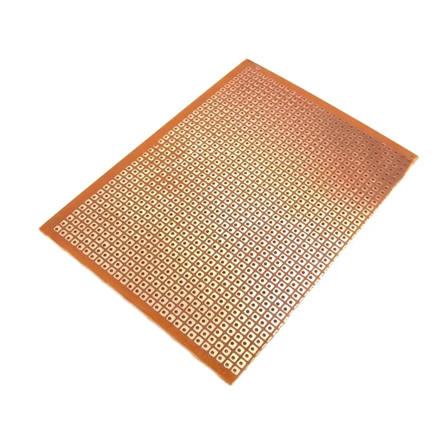
A Zero PCB, often referred to as a perfboard or protoboard, is a fundamental type of circuit board characterized by a grid of holes, typically featuring copper pads around each hole. Unlike standard printed circuit boards (PCBs), a Zero PCB lacks any pre-defined conductive tracks or circuit patterns. Its primary function is to provide a versatile platform for the manual assembly and testing of electronic circuits. Components are placed and connected by soldering or wiring, creating custom circuits as needed.
Key characteristics of a Zero PCB include:
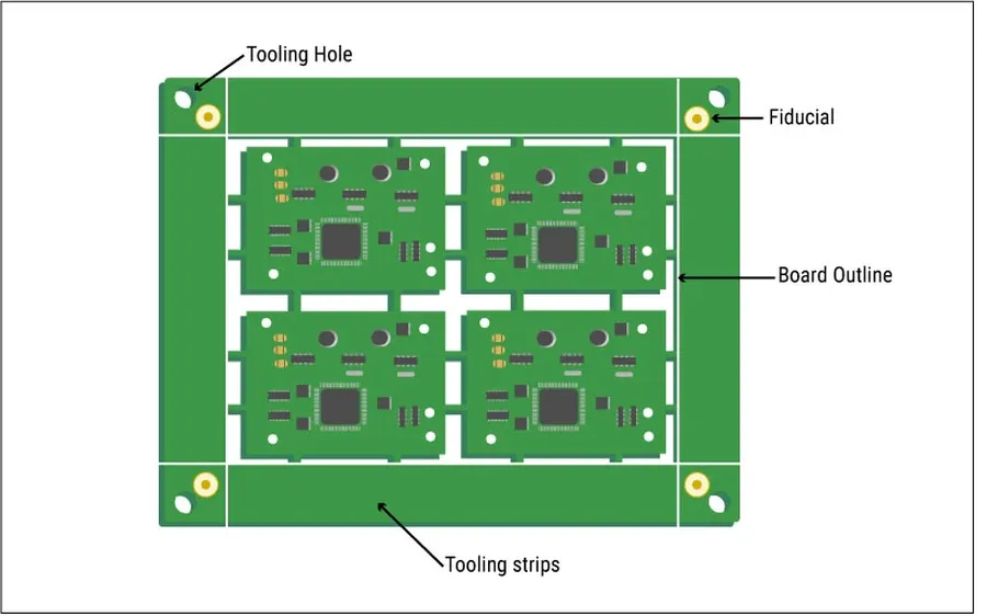
Zero PCBs, also referred to as perfboards or protoboards, stand in stark contrast to standard Printed Circuit Boards (PCBs) in their design, application, and manufacturing process. Unlike standard PCBs, which are meticulously engineered for specific circuit designs, zero PCBs provide a versatile platform for manual circuit construction and prototyping. This fundamental difference leads to a variety of distinctions in their usage and advantages.
| Feature | Zero PCB | Standard PCB |
|---|---|---|
| Circuit Design | Universal grid of holes, no predefined tracks | Custom-designed with specific circuit patterns |
| Manufacturing | No manufacturing process; manual assembly required | Requires professional fabrication with etching and plating processes |
| Assembly | Manual component placement and wiring | Automated component placement and soldering is typical |
| Flexibility | Highly flexible for modifications and experimentation | Limited flexibility after design is finalized |
| Cost | Lower cost, ideal for prototyping and small projects | Higher cost, especially for custom designs and small production runs |
| Prototyping | Ideal for quick and low-cost prototyping | Not ideal for iterative prototyping |
| Production | Not suitable for mass production | Suitable for mass production with consistent quality |
| Permanence | Solderable connections offer a semi-permanent construction | Highly permanent connections |
The selection between a zero PCB and a standard PCB hinges largely on the project requirements, encompassing factors like budget, project stage, and the volume of production. Zero PCBs are favored during the early stages of design and prototyping due to their inherent flexibility and cost-effectiveness. Conversely, standard PCBs become the preferred choice once the design has been finalized and requires high precision and a more streamlined manufacturing process for final product development or mass production.
Zero PCBs, while seemingly simple, come in several varieties, each suited to different prototyping needs. Understanding these variations is crucial for selecting the most appropriate board for your project, ensuring both efficiency and effectiveness in your design process. The key differentiators include the number of conductive layers, the presence or absence of plated through-holes, and the grid pattern.
| Type | Description | Typical Use Cases | Advantages | Disadvantages |
|---|---|---|---|---|
| Single-Sided Zero PCB | Has copper traces on one side only. | Simple circuits, educational projects | Lower cost, easier to work with | Limited complexity, difficult for high-density projects |
| Double-Sided Zero PCB | Has copper traces on both sides. | More complex circuits, medium-density projects | Increased routing options, higher component density | Slightly more difficult to solder, requires more care |
| Zero PCB with Plated Through-Holes | Holes are plated with conductive material, allowing connections between layers. | Circuits requiring multiple layers connections, more robust designs | Facilitates easier soldering and component connection, allows for vertical stacking of components | Slightly more expensive |
| Zero PCB without Plated Through-Holes | Holes are not plated, connections are limited to the same side. | Simple circuits where all connections can be made on one side | Lowest cost, simple manufacturing process | More challenging to make inter layer connections |
| Various Grid Patterns | Common grid patterns including 2.54mm (0.1-inch) and sometimes smaller. | Varying component sizes and mounting options | Flexibility in component choice | May require specific adapters for non-standard components |
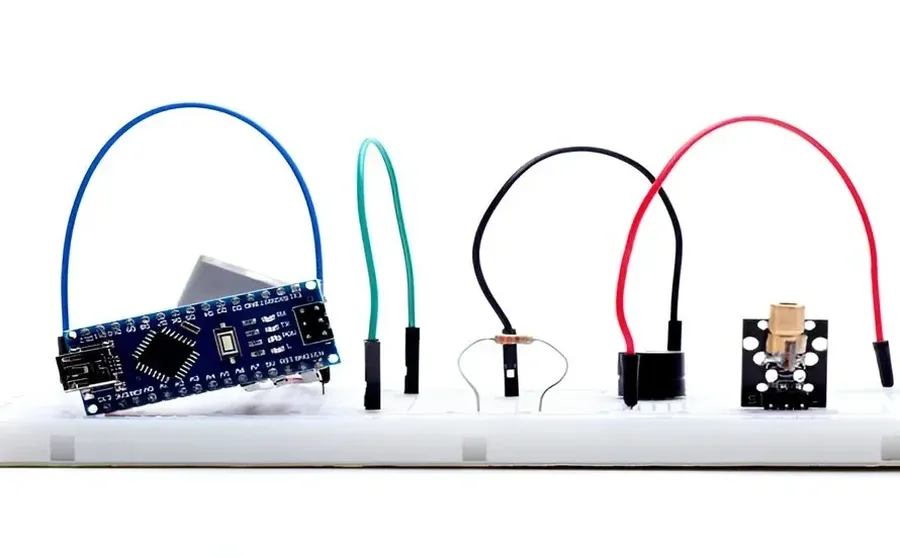
Constructing a circuit on a zero PCB, also known as perfboard or protoboard, involves the manual placement of electronic components and the creation of electrical connections using soldering, wires, or jumpers. Unlike standard PCBs with pre-etched conductive tracks, zero PCBs require the user to manually establish all circuit paths, providing maximum flexibility during the prototyping phase.
| Aspect | Zero PCB | Standard PCB |
|---|---|---|
| Circuit Path Creation | Manual connections via soldering, wires | Pre-defined copper tracks |
| Flexibility | High flexibility for modifications | Limited flexibility after manufacturing |
| Cost | Lower cost for small batches/prototypes | Higher cost for manufacturing |
| Prototyping | Ideal for prototyping and experimentation | Not ideal for iterative prototyping |
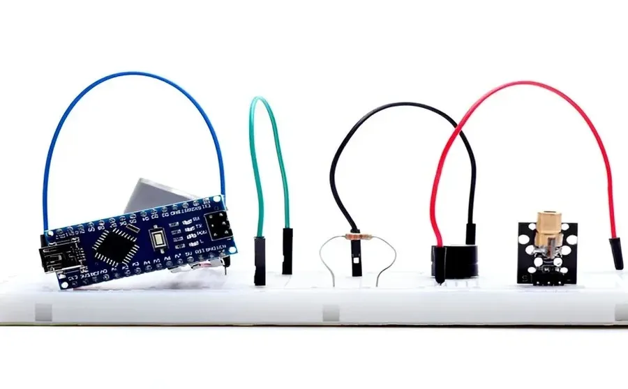
Zero PCBs, celebrated for their adaptability and cost-effectiveness, find extensive use across diverse applications, particularly in prototyping, educational environments, and DIY electronics. Their key advantage lies in enabling rapid circuit design testing without the delays or financial burdens associated with custom PCB manufacturing.
| Feature | Zero PCB | Custom PCB |
|---|---|---|
| Cost | Low | High |
| Flexibility | High | Low |
| Lead Time | Immediate | Longer |
| Modification | Easy | Difficult |
| Ideal Use | Prototyping, DIY, Education | Mass Production |
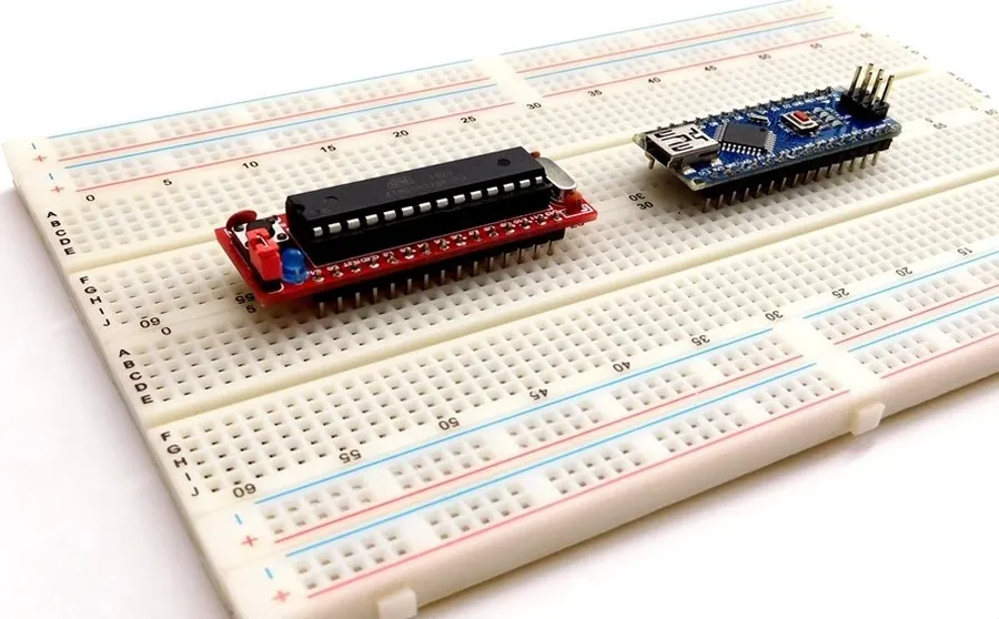
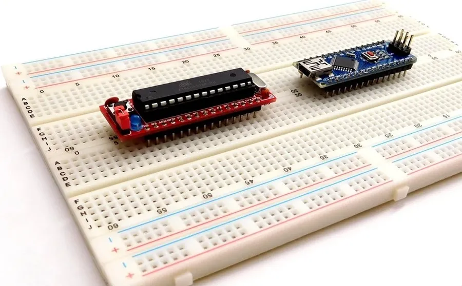
Zero PCBs and breadboards are both utilized for electronic prototyping, but they cater to different needs and project stages. Zero PCBs offer a more permanent and robust solution through soldering, while breadboards provide a temporary, solderless platform for rapid testing and experimentation.
| Feature | Zero PCB | Breadboard |
|---|---|---|
| Connectivity | Permanent connections via soldering | Temporary connections via spring clips |
| Durability | Robust and suitable for permanent circuits | Less durable and prone to loose connections |
| Component Mounting | Components are soldered directly onto the board | Components are inserted into breadboard's terminal strips |
| Circuit Stability | Provides a more stable and reliable circuit | Less stable due to temporary connections |
| Complexity | Suitable for more complex and permanent circuits | Ideal for simple circuits and quick testing |
| Cost | Relatively low cost for the board itself, but requires soldering equipment and materials | Low initial cost, no soldering equipment needed |
| Reusability | Less reusable once components are soldered | Highly reusable for multiple projects |
| Modification | Modifications are more complex and require desoldering | Easy to modify and reconfigure circuits |
This section addresses common inquiries regarding Zero PCBs, providing clarity on their applications, capabilities, and cost-effectiveness. Understanding these FAQs will help clarify the role of Zero PCBs in electronics prototyping and development, especially when compared with standard PCBs and breadboards.
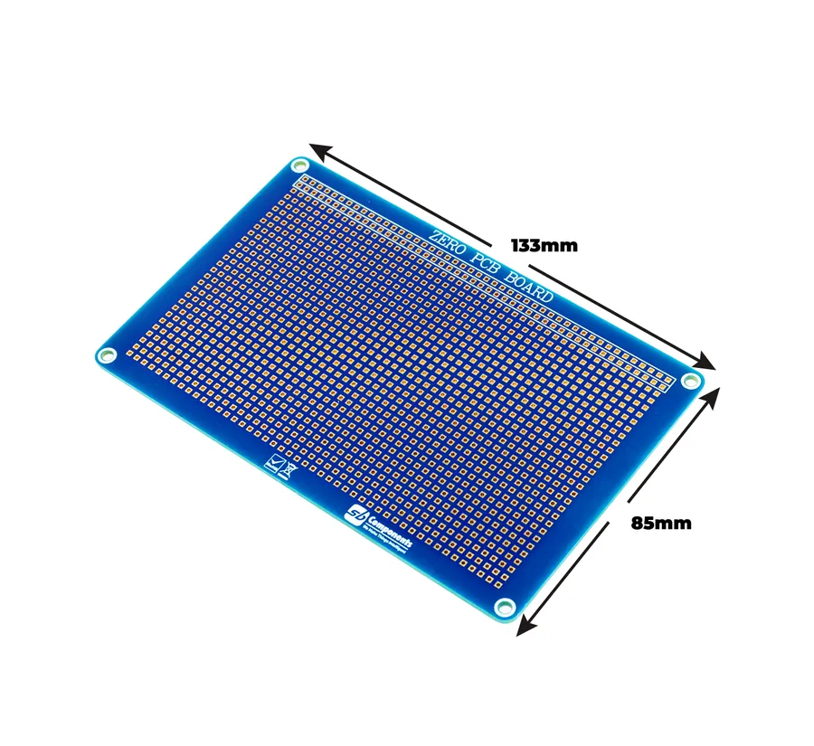
This practical guide provides beginners with the essential steps and techniques for creating robust and long-lasting prototypes using zero PCBs. Emphasis is placed on proper soldering techniques, selecting appropriate components and layouts, and implementing design considerations that result in a stable and reliable circuit.
In conclusion, the Zero PCB stands as a cornerstone in the world of electronics, offering a flexible and cost-effective solution for prototyping and circuit development. Its versatility and ease of use make it an invaluable tool for beginners and experienced designers alike. Understanding its characteristics, applications, and differences from other prototyping methods enables users to maximize their project potential. When considering project design and testing, the Zero PCB offers a unique blend of flexibility, robustness and accessibility without the zero PCB cost, making it a critical resource in the development of new circuits.

