In the world of electronics, the transistor is a fundamental building block, much like the heart in the human body. The BC547 NPN transistor, a small yet powerful component, plays a crucial role in countless devices, from simple switches to sophisticated amplifiers. This article delves into the inner workings of the BC547, providing an accessible understanding of its operation and applications. Let's discover how the BC547 bridges the gap between theoretical concepts and practical electrical engineering, demonstrating how a basic silicon structure can power much of the modern electronic world.
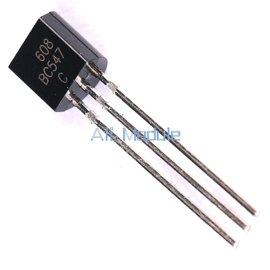
The BC547 is a fundamental NPN Bipolar Junction Transistor (BJT) widely used in electronic circuits. Its core function relies on controlling current flow between the collector and emitter terminals using a small current applied to the base. This three-terminal device – collector, base, and emitter – is essential for amplification and switching operations in numerous electronic applications.
The BC547's structure consists of three semiconductor layers: a P-doped layer sandwiched between two N-doped layers, creating two PN junctions. The collector and emitter regions are N-type, while the base region is P-type. This NPN structure dictates its operational characteristics and biases the transistor for use in a specific manner.
Operationally, a small current injected into the base terminal influences a larger current flowing between the collector and emitter. This amplification ability is key to its use in a wide variety of applications. Understanding this principle is critical for designing functional transistor circuits.
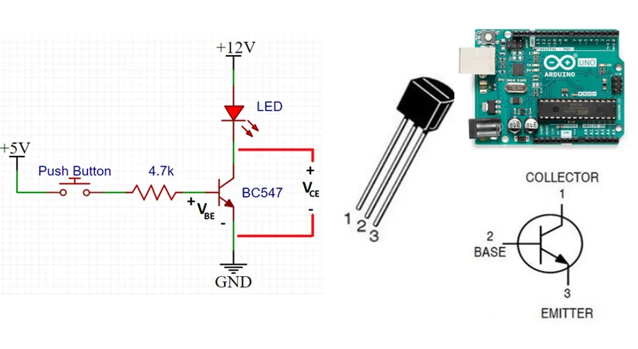
The BC547 is a three-terminal NPN bipolar junction transistor (BJT), and understanding its pinout is crucial for proper integration into electronic circuits. The three pins are the collector (C), the base (B), and the emitter (E). Correctly identifying each of these pins and their orientation is essential for the transistor to function as intended, whether as a switch or amplifier.
| Pin | Description | Function |
|---|---|---|
| Collector (C) | Typically the pin where current flows into the transistor. | Receives the primary current flow when the transistor is active. |
| Base (B) | The pin used to control the current flow between the collector and emitter. | Controls the transistor's on/off state and the amount of current flowing. |
| Emitter (E) | Typically the pin where current flows out of the transistor. | The reference point from which the primary current flows out when the transistor is active. |
When viewing the BC547 with the flat side facing you and the pins pointing downwards, the pinout, from left to right is: emitter (E), base (B), and collector (C). It is imperative to confirm the correct orientation before connecting it to a circuit to avoid damage.
Understanding the electrical characteristics of the BC547 NPN transistor is crucial for its effective implementation in circuit design. These specifications dictate the performance limits and operational parameters of the transistor, ensuring it functions as intended within various applications. Key parameters include maximum collector current, collector-emitter voltage, DC current gain (hFE), and power dissipation.
| Parameter | Symbol | Value | Unit | Description |
|---|---|---|---|---|
| Maximum Collector Current | IC(max) | 100 | mA | The maximum current that the transistor can handle safely through the collector terminal. |
| Collector-Emitter Voltage | VCE(max) | 45 | V | The maximum voltage that can be applied between the collector and emitter terminals without causing damage. |
| Collector-Base Voltage | VCB(max) | 50 | V | The maximum voltage that can be applied between the collector and base terminals without causing damage. |
| Emitter-Base Voltage | VEB(max) | 6 | V | The maximum voltage that can be applied between the emitter and base terminals without causing damage. |
| DC Current Gain | hFE | 110-800 (typical) | - | The ratio of collector current to base current. This parameter determines the transistor's amplification capabilities; the typical range indicates variations between different devices. |
| Power Dissipation | PD(max) | 625 | mW | The maximum power the transistor can dissipate without overheating. This value is typically under specific ambient temperature conditions. |
| Transition Frequency | fT | 300 | MHz | The frequency at which the current gain of the transistor drops to unity. |
These specifications are crucial for ensuring the BC547 operates within its safe operating area (SOA). Exceeding these values can lead to device failure. The hFE, for example, is a critical factor when using the BC547 as an amplifier or in switching circuits. A higher hFE allows the transistor to achieve a higher current gain with a relatively low base current. Power dissipation should be carefully managed to prevent thermal runaway and component damage. Datasheets from manufacturers like ON Semiconductor or NXP provide comprehensive data on these and other parameters, including temperature coefficients, which should be considered for accurate circuit analysis and design. Understanding these parameters enables designers to select the right transistor for a specific application and to ensure optimal performance and reliability of electronic circuits.
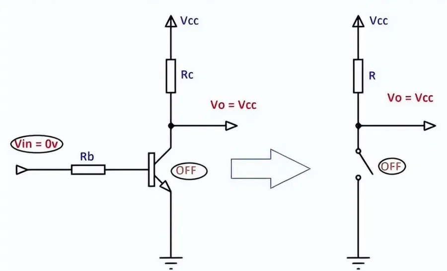
The BC547 NPN transistor excels as an electronic switch by leveraging its ability to rapidly transition between conductive (saturation) and non-conductive (cutoff) states, controlled by a current applied to its base terminal. This behavior makes it suitable for many digital logic and power control applications.
The key to understanding how the BC547 operates as a switch lies in the concept of saturation and cutoff. In the saturation region, the transistor behaves like a closed switch, allowing maximum current to flow between the collector and emitter. Conversely, in the cutoff region, the transistor behaves like an open switch, blocking current flow. Transition between these two states is controlled by a small base current.
| State | Base Current (Ib) | Collector Current (Ic) | Collector-Emitter Voltage (Vce) | Transistor Behavior |
|---|---|---|---|---|
| Cutoff | Ib ≈ 0 | Ic ≈ 0 | Vce ≈ Vcc | Open switch |
| Saturation | Ib ≥ Ib(sat) | Ic ≈ Ic(max) | Vce ≈ Vce(sat) ≈ 0.2 V | Closed switch |
To switch the BC547 into saturation, a sufficient base current (Ib) must be supplied. The minimum base current required can be calculated based on the desired collector current (Ic) and the transistor's current gain (hFE): Ib(sat) ≈ Ic(max) / hFE. When the base current is sufficient, the transistor moves into saturation, allowing a current from the collector to the emitter. When the base current is removed, the transistor enters the cutoff region, blocking the current flow.
Simple switching circuit example: A typical use case involves controlling an LED. The base of the BC547 is connected to a digital output through a resistor (Rb), the emitter is connected to the ground, and the collector is connected to an LED, which is also connected to a voltage source through a resistor (Rc). When the digital output provides a voltage (a HIGH signal), current flows from the digital pin, through the base resistor Rb, and into the base of the BC547, causing the transistor to switch to saturation, thus turning on the LED. When the digital output is LOW, no current flows into the base, putting the transistor into cutoff mode, turning off the LED.
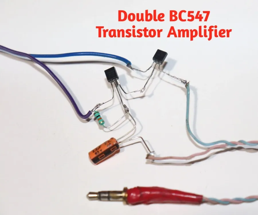
The BC547 transistor's ability to amplify electrical signals makes it a valuable component in numerous electronic circuits. When configured as an amplifier, the BC547 leverages its inherent capacity to modulate a larger current at the collector-emitter terminals by a smaller current at the base, thus achieving signal amplification.
A typical amplification configuration is the common-emitter amplifier. In this setup, the input signal is applied to the base terminal, the amplified output is taken from the collector, and the emitter is connected to the common reference point, usually ground. The key performance characteristic of the BC547 as an amplifier is its current gain, often represented as hFE or β, which quantifies the relationship between collector current and base current. This parameter is not a constant and varies with operating conditions and temperature.
Achieving optimal performance from the BC547 amplifier hinges on proper biasing. Biasing refers to setting the DC operating point of the transistor to a region that allows for amplification without distortion. Improper biasing can lead to signal clipping or loss of amplification. A common method of biasing the BC547 is using a voltage divider network at the base and a collector resistor, which establishes a stable operating point irrespective of the transistor's hFE variability. The bias point should position the transistor in the active region, where the relationship between base current and collector current is essentially linear.
| Parameter | Description | Typical Effect on Amplification |
|---|---|---|
| Current Gain (hFE) | Ratio of collector current to base current | Higher hFE values provide greater amplification. |
| Collector Resistor | Sets the voltage gain and load for the amplifier | Higher resistance increases voltage gain but may limit current. |
| Bias Resistors | Establish the DC operating point of the transistor | Incorrect values can lead to signal distortion. |
| Input Impedance | Resistance presented at the input terminal | Affects how effectively the amplifier draws signal from the source. |
| Output Impedance | Resistance presented at the output terminal | Influences how effectively the amplifier delivers signal to the load. |
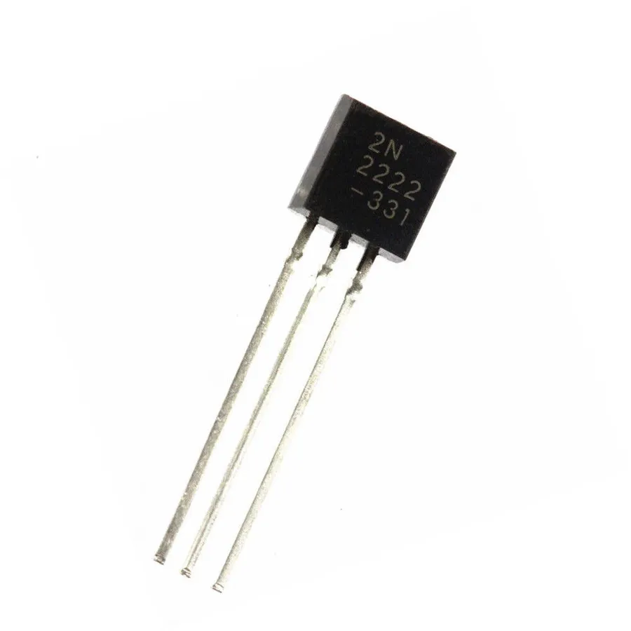
While the BC547 is a widely used NPN transistor, several other transistors can serve as equivalents or substitutes. Understanding the nuances between the BC547 and its alternatives, such as the BC548, BC549, and BC550, is essential for effective circuit design and troubleshooting. This section explores their key differences and interchangeability.
| Feature | BC547 | BC548 | BC549 | BC550 |
|---|---|---|---|---|
| Maximum Collector Current (Ic max) | 100mA | 100mA | 100mA | 100mA |
| Collector-Emitter Voltage (Vce max) | 45V | 30V | 30V | 50V |
| DC Current Gain (hFE) Range | 110-800 | 110-800 | 200-800 | 200-800 |
| Transition Frequency (fT) | 300MHz | 300MHz | 300MHz | 300MHz |
| Noise Figure | Low | Low | Very Low | Very Low |
| Application Notes | General purpose | General purpose | Low noise | Low noise |
The BC548 is a very close equivalent to the BC547, often considered interchangeable in most applications. The primary difference lies in the maximum collector-emitter voltage (Vce), where the BC547 has a slightly higher rating (45V) than the BC548 (30V). For general-purpose applications not exceeding 30V, they can be used interchangeably.
The BC549 and BC550 are also similar to the BC547, but they are typically used in applications where low noise is critical. The BC549 and BC550 offer significantly lower noise characteristics compared to the BC547 and BC548, making them ideal for audio amplification and sensitive sensor applications. Furthermore, their higher hFE typically makes them more sensitive to input currents. Similar to the voltage differences between the BC547 and BC548, the BC550 is a slightly more robust version of the BC549 with a higher Vce rating of 50V.
When selecting a substitute, consider the application's specific requirements. If the circuit requires low noise, the BC549 or BC550 are more suitable alternatives. If the circuit operates at a voltage close to or above 30V but below 45V, the BC547 is better than the BC548. When the circuit operates in very low voltage and current requirements, BC549 or BC550 are suitable candidates due to higher hFE
In essence, while these transistors share many similarities, their differences—particularly in terms of noise performance, gain, and voltage handling capabilities—dictate the most appropriate choice for a given application. It's always prudent to consult the datasheets for precise specifications before making a substitution.
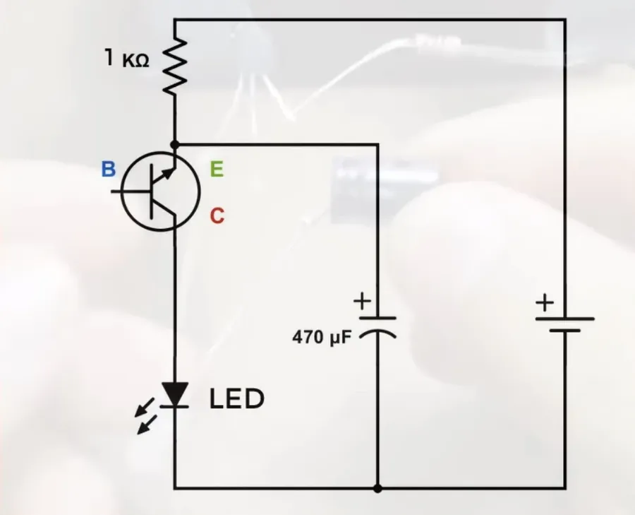
The BC547 NPN transistor's versatility is demonstrated through its wide array of applications. Its ability to function as both a switch and an amplifier makes it a fundamental component in numerous electronic circuits. These applications span from basic control mechanisms to more complex amplification stages.
| Application | Description | Circuit Type |
|---|---|---|
| LED Control | Switching an LED on/off | Switching |
| Small Motor Control | On/off control of a small DC motor | Switching |
| Light Activated Relay | Activating a relay based on light | Switching |
| Audio Pre-Amplification | Boosting the voltage of a weak audio signal | Amplification |
| Simple Signal Shaper | Shaping signals for various circuit requirements | Signal Processing |
This section addresses common questions regarding the BC547 NPN transistor, providing concise answers to enhance understanding of its functionality and applications.
The BC547 NPN transistor stands out as a fundamental component in electronics, due to its versatility and widespread availability. From basic switching applications to signal amplification, the BC547 plays a crucial role. Its simplicity and reliability make it an ideal component for both beginners and experienced engineers. Understanding the principles of how this transistor operates provides invaluable insights into the vast world of electronics. The BC547 transistor serves not only as a practical tool, but also as a gateway to understanding complex electrical systems, highlighting its importance in the development of modern electronics.

