In the intricate dance of electronics, the 4-layer PCB emerges as a versatile workhorse, bridging the gap between simplicity and sophistication. Much like the layers of a carefully crafted cake, a 4-layer PCB balances signal integrity, power distribution, and cost-effectiveness, making it a cornerstone of countless modern devices. This article delves into the heart of 4-layer PCB technology, revealing its construction, design nuances, and the wide array of applications that rely on its capabilities, empowering you to understand and effectively utilize this essential component.
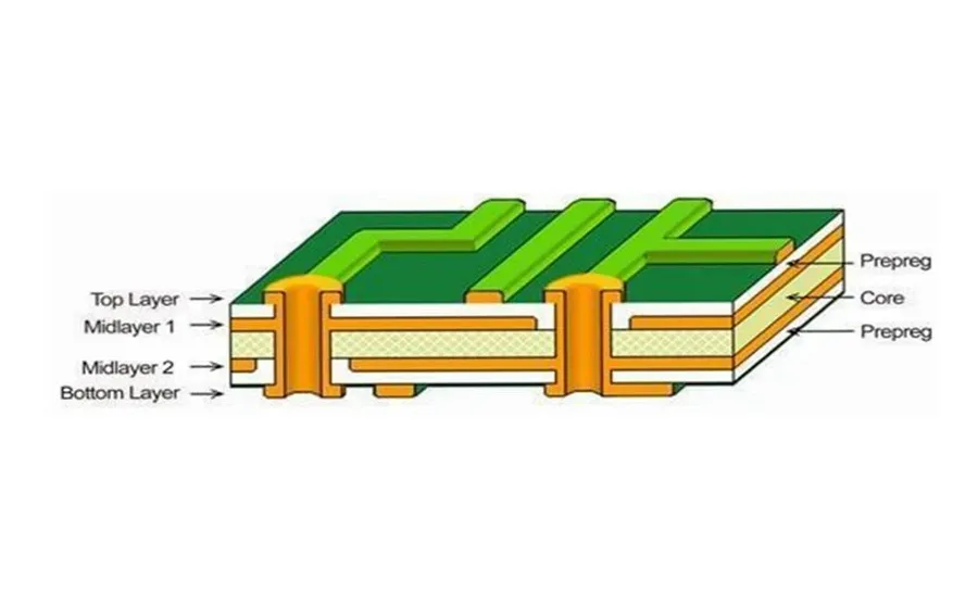
A 4-layer Printed Circuit Board (PCB) is constructed with four distinct layers of conductive material, typically copper, separated by insulating dielectric material. This arrangement provides a balance between complexity and performance, making them suitable for a wide range of electronic applications. Understanding the specific arrangement and purpose of each layer is fundamental to effective PCB design.
In a typical 4-layer PCB stackup, the layers are often allocated as follows: * **Top Layer (Signal Layer):** This outermost layer is used for routing signal traces and placing components. * **Inner Layer 1 (Ground Plane):** This layer serves as a dedicated ground plane, providing a low-impedance return path for signals. This is critical for minimizing signal noise and interference. * **Inner Layer 2 (Power Plane):** This layer acts as a power plane, distributing power to the various components on the board. * **Bottom Layer (Signal Layer):** This outermost layer, similar to the top layer, is also used for routing signals and placing components.
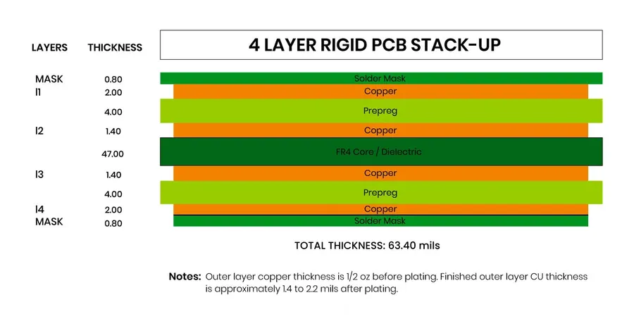
The stackup of a 4-layer PCB is paramount to its overall performance, influencing signal integrity, impedance control, and electromagnetic compatibility (EMC). A well-defined stackup strategically arranges the signal, power, and ground layers to optimize signal transmission and minimize noise.
Common 4-layer PCB stackup configurations typically involve a signal layer on the top and bottom surfaces, with a ground plane and a power plane in the inner layers. This arrangement creates a defined impedance for signal traces, essential for high-speed designs. Variations in stackup might include having two signal layers adjacent or splitting the power plane into multiple voltage rails to reduce the need for multiple power layers. Selecting an appropriate stackup is not arbitrary; it requires a deep understanding of the specific functional and performance requirements of the board, such as signal frequency, power needs, and sensitivity to noise.
| Stackup Type | Description | Advantages | Disadvantages | Use Cases |
|---|---|---|---|---|
| Signal-Ground-Power-Signal | The most common configuration, with two outer signal layers, an inner ground layer, and an inner power layer. | Good impedance control, simplified routing, good noise performance. | Limited routing flexibility on inner layers, less space for power distribution. | General-purpose applications, medium-speed circuits, sensors, data acquisition |
| Signal-Power-Ground-Signal | Outer signal layers, followed by a power plane and a ground plane in the middle. | Reduced DC resistance in power distribution, improved power integrity. | May increase overall thickness, slightly more complex routing. | High-power circuits, analog circuits, where power delivery is important. |
| Signal-Signal-Ground-Power | Two outer signal layers, followed by inner ground and power layers. | Good for high-speed signal routing on the outer layers, suitable for controlled impedance applications | May result in less effective EM shielding and increased power noise. | High-speed digital circuits where signal integrity is a priority |
The chosen stackup directly impacts the signal integrity by defining the signal path and controlling the impedance. For instance, placing a ground plane close to a signal layer creates a controlled impedance environment, reducing signal reflections and ensuring accurate signal transmission. An incorrect stackup can lead to impedance mismatches, signal reflections, and increased EMI (Electromagnetic Interference), compromising overall system performance. Therefore, a carefully considered stackup is the foundation of a successful 4-layer PCB design.
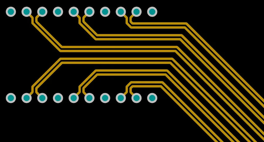
Achieving controlled impedance, particularly the common 50-ohm target, is paramount in 4-layer PCB design to ensure signal integrity and minimize signal reflections. This requires careful consideration of the layer stackup, trace dimensions, and dielectric material properties. A well-designed stackup minimizes impedance variations, resulting in high performance and signal integrity.
| Parameter | Description | Impact on Impedance |
|---|---|---|
| Trace Width | The width of the signal trace on the PCB layer. | Wider traces generally lower impedance. |
| Trace Thickness | The thickness of the copper trace. | Thicker traces generally lower impedance. |
| Trace Spacing | The distance between signal traces and adjacent ground/power planes. | Closer spacing to ground planes lowers impedance. |
| Dielectric Height | The thickness of the dielectric material between layers. | Thinner dielectric material generally lowers impedance. |
| Dielectric Constant | A measure of the ability of a material to store electrical energy. | Higher dielectric constant lowers impedance. |
To achieve a 50-ohm impedance, it's necessary to use impedance calculation tools or simulation software. These tools account for the intricate interplay of the parameters mentioned above. A typical microstrip configuration, where a signal trace is on an outer layer with a ground plane beneath it, or a stripline configuration, where a signal trace is embedded between two ground planes, will be used. The choice between these depends on the design and interference factors.
Furthermore, beyond 50-ohm impedance, other specific impedance requirements may exist for certain signals, such as differential pairs. These require meticulous design considerations. Utilizing impedance control techniques during the PCB design phase is essential to ensure that the PCB operates within the required specifications, ensuring consistent signal performance. Impedance control is not just a design feature but an integral part of the fabrication process, where each layer's copper thickness and dielectric separation needs to be consistent to achieve the desired results.
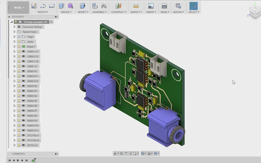
Effective 4-layer PCB design hinges on adherence to key guidelines that ensure both functionality and reliability. These guidelines encompass routing strategies, component placement, and the appropriate use of vias to manage signal integrity, power distribution, and thermal characteristics.
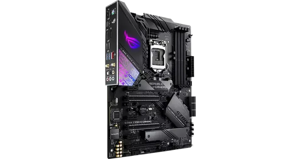
4-Layer PCBs strike a balance between cost, complexity, and performance, making them suitable for a wide array of applications across various industries. Their multi-layer structure allows for effective routing of signals and power, alongside dedicated ground planes, crucial for modern electronics.
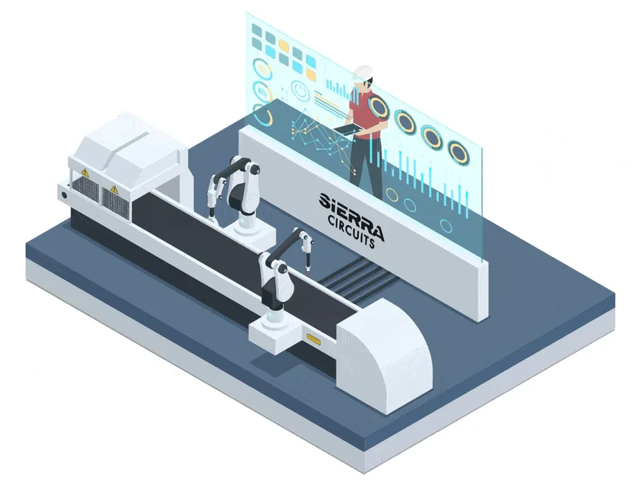
The fabrication of 4-layer PCBs is a sophisticated process involving multiple stages, transforming raw materials into functional circuit boards. This process demands precision and adherence to strict quality control measures to ensure reliable performance.
The cost of a 4-layer PCB is determined by a multitude of factors, primarily revolving around material choices, design complexity, and production volume. Understanding these cost drivers is crucial for effective budget management in electronics projects. By carefully considering each aspect, you can optimize your design for cost efficiency without compromising performance.
| Cost Factor | Description | Impact on Cost |
|---|---|---|
| Material Selection | The type of substrate material (e.g., FR-4, polyimide), copper thickness, and finish (e.g., HASL, ENIG) directly affect the price. | Higher performing materials and finishes increase the cost. For example, ENIG is more expensive than HASL. |
| PCB Size and Dimensions | The overall size and dimensions of the PCB impact material usage and production time. | Larger boards consume more material and may require more complex handling in manufacturing, increasing the cost. |
| Design Complexity | Factors such as the number of vias, trace density, fine-pitch components, and special features increase manufacturing difficulty. | More complex layouts require precise manufacturing processes, leading to higher costs. |
| Layer Count | While this section focuses on 4-layer PCBs, the number of layers is a primary cost driver. | Each additional layer increases material cost and manufacturing complexity, which increases price over a 2 layer board. |
| Production Volume | The quantity of PCBs produced in a single run affects the unit price. | Higher production volumes usually result in lower per-unit costs due to economies of scale. |
| Manufacturing Process | Specific manufacturing requirements such as laser drilling, blind or buried vias can affect price. | Specialized processes usually incur a premium. |
| Testing and Quality Control | Thorough electrical testing and inspection of the boards. | Advanced testing or specialized tests increases cost. |
This section addresses common questions about 4-layer PCBs, providing clarity on their design, stackup, routing, and application. These FAQs aim to resolve typical user concerns and enhance understanding.
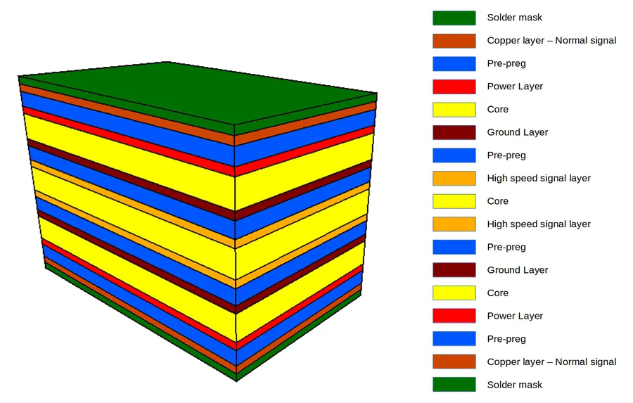
Understanding the nuances between different PCB layer counts is crucial for selecting the right board for your project. This section provides a comparative analysis of 4-layer PCBs against 2-layer and 6-layer PCBs, highlighting their respective strengths and limitations to inform your design choices.
| Feature | 2-Layer PCB | 4-Layer PCB | 6-Layer PCB |
|---|---|---|---|
| Complexity | Simplest, suitable for basic circuits. | Moderate complexity, balance of performance and cost. | Higher complexity, for advanced applications. |
| Cost | Lowest cost. | Moderate cost. | Higher cost. |
| Routing Flexibility | Limited, routing on two layers only. | Improved, with dedicated power/ground planes and signal routing layers | Most flexible, with additional signal layers for complex layouts. |
| Signal Integrity | Most susceptible to noise and signal degradation. | Better performance with dedicated power/ground planes to reduce EMI and crosstalk. | Highest performance with multiple signal layers and tightly controlled impedance. |
| Power Distribution | More challenging, requires wide traces. | Good power distribution through dedicated power planes. | Excellent power distribution capabilities with multiple power planes. |
| Size and Density | Lower density due to limited routing. | Moderate density, suitable for many applications. | Highest density to accommodate complex circuits. |
| Applications | Simple consumer electronics, hobbyist projects. | Many electronic devices, including power supplies and microcontroller boards. | High-performance devices, communication systems, and advanced computing. |
| Impedance Control | Basic impedance control is more challenging. | Good impedance control through stack-up selection and plane utilization. | Excellent impedance control for high speed signals and RF applications. |
The 4-layer PCB stands as a testament to the ingenuity of modern electronics, providing a robust and versatile platform for a myriad of applications. From the intricate layout of a smartphone to the robust control system of an industrial robot, the 4-layer PCB's careful balance of signal management, power distribution, and cost-effectiveness makes it an indispensable component. Whether you are designing your first circuit board or a seasoned engineer optimizing complex layouts, understanding the nuances of 4-layer PCB design is key to unlocking its full potential. The insights and guidelines discussed in this article will serve as a valuable starting point for your journey into the world of 4-layer PCBs, enabling you to confidently tackle design challenges and create innovative, reliable electronic systems.

