In the realm of electronics, the 2N3904 transistor stands as a ubiquitous component, much like the basic building blocks of our modern world. From the smallest embedded system to the sophisticated control circuits, the 2N3904 NPN transistor plays a key role as a switch and amplifier. This article will delve into the inner workings of this essential semiconductor, illuminating its characteristics, practical uses, and alternatives, empowering hobbyists and professionals alike to make the most of its capabilities. We'll start by understanding the basic function of the 3904 transistor and then dive into more specifics.
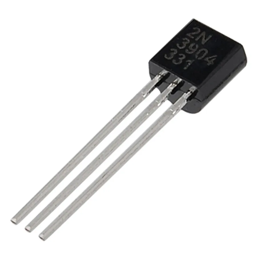
The 2N3904 is a ubiquitous NPN Bipolar Junction Transistor (BJT) that serves as a fundamental building block in countless electronic circuits. Its core function is to act as a current-controlled switch or amplifier. The NPN designation signifies that the transistor comprises a layer of P-type semiconductor material sandwiched between two layers of N-type semiconductor material. This structure enables the 2N3904 to regulate current flow between its collector and emitter terminals based on the current applied to its base terminal.
| Feature | Description |
|---|---|
| Type | NPN Bipolar Junction Transistor (BJT) |
| Material | Silicon |
| Basic Function | Current-controlled switch and amplifier |
| Structure | N-P-N layers |
| Control Terminal | Base |
In its role as a switch, the 2N3904 can be used to turn a circuit on or off, where a small base current can control a significantly larger collector current. As an amplifier, the 2N3904 can boost weak electrical signals, making them usable for various applications, such as audio amplification or sensor signal processing. The functionality of the 2N3904 stems from the behavior of charge carriers (electrons and holes) within the semiconductor layers when a small current is applied to the base.
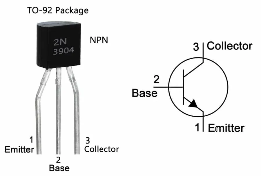
The 2N3904 transistor is typically housed in a TO-92 package, a widely used, cost-effective, and easily handled through-hole package. This package features three leads, each corresponding to one of the transistor's three terminals: the base, collector, and emitter. Correct identification and connection of these terminals are crucial for the proper operation of any circuit utilizing the 2N3904.
| Pin Number | Pin Name | Description | Polarity |
|---|---|---|---|
| 1 | Emitter (E) | The terminal from which current flows out of the transistor. | Negative or reference terminal for NPN BJT operation. |
| 2 | Base (B) | The control terminal. A small current applied here modulates the current flow between collector and emitter. | Positive terminal for NPN BJT operation. |
| 3 | Collector (C) | The terminal into which current flows into the transistor. | Positive terminal for NPN BJT operation. |
The physical orientation of the TO-92 package when looking at the flat face, the leads are arranged from left to right as Emitter, Base, and Collector. It is important to note that the TO-92 package may appear slightly different between manufacturers, it is always best practice to consult the component's datasheet to ensure proper pin identification.
The 2N3904 transistor, a widely used NPN Bipolar Junction Transistor (BJT), is characterized by several key specifications that dictate its performance in electronic circuits. These parameters, typically found in the device datasheet, are essential for engineers to understand when designing and using the transistor for various applications such as switching and amplification.
| Parameter | Symbol | Typical Value | Conditions | Unit |
|---|---|---|---|---|
| Collector-Emitter Breakdown Voltage | VCEO | 40 | Ic = 1 mA, Ib = 0 | V |
| Collector-Base Breakdown Voltage | VCBO | 60 | Ic = 100 μA, Ie=0 | V |
| Emitter-Base Breakdown Voltage | VEBO | 6 | Ie = 100 μA, Ic=0 | V |
| Maximum Collector Current | Ic(max) | 200 | Continuous | mA |
| Maximum Power Dissipation | PD(max) | 625 | TA=25°C | mW |
| DC Current Gain | hFE | 100-300 | Ic = 10 mA, Vce = 1V | - |
| Collector-Emitter Saturation Voltage | VCE(sat) | 0.2 | Ic=10mA, Ib=1mA | V |
| Transition Frequency | fT | 300 | Ic=10mA, Vce = 10V | MHz |
Understanding these specifications is crucial for effective circuit design. For instance, the maximum collector current (Ic(max)) determines the maximum load the transistor can handle, while the current gain (hFE) indicates the transistor's amplification capability. The saturation voltage (VCE(sat)) is important when using the transistor as a switch, as it dictates the voltage drop across the transistor when fully turned on. Additionally, the transition frequency (fT) specifies the maximum frequency at which the transistor can effectively amplify or switch signals.
It is imperative to consult the specific manufacturer's datasheet for precise specifications, as these values can vary slightly between manufacturers and production batches. Deviating from these recommended operating conditions may result in reduced performance or damage to the device. It is always advisable to operate the transistor within its safe operating area.
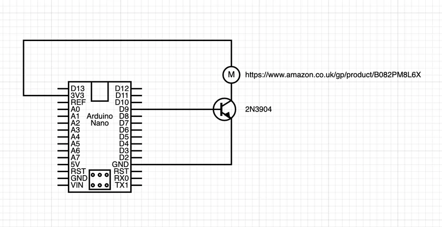
The 2N3904 transistor, a ubiquitous NPN Bipolar Junction Transistor (BJT), is frequently employed as an electronic switch. Its ability to control current flow based on a small input signal makes it ideal for switching applications, effectively turning on or off circuits to power various loads.
In a typical switching configuration, the 2N3904 operates in two primary states: saturation and cutoff. In saturation, a sufficient base current allows maximum current to flow from the collector to the emitter, effectively closing the switch. Conversely, in cutoff, no base current flows, preventing current flow between the collector and the emitter, thus opening the switch. This behavior allows the transistor to act as a controlled on-off mechanism, manipulating power to the desired load.
The control signal, applied to the base terminal, allows the 2N3904 to switch larger currents than what is applied to the base. This current amplification is a key advantage of BJTs, allowing them to be used to drive loads with modest input signals. When using a 2N3904 as a switch, it's vital to select the appropriate base resistor to limit the base current, ensuring that the transistor saturates correctly and avoids damage.
| Application | Load Type | Considerations |
|---|---|---|
| LED Control | Resistive | Choose appropriate base resistor to saturate the transistor, but limit base current. |
| Relay Control | Inductive | Include a flyback diode across the relay coil to prevent voltage spikes. |
| Motor Control | Inductive | Use of flyback diodes recommended, heat-sinking may be required for larger current motors |
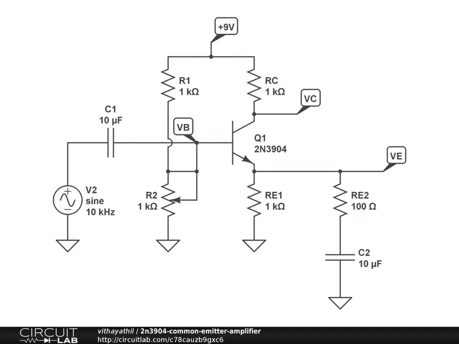
The 2N3904 transistor, beyond its switching capabilities, serves as a fundamental building block for low-power amplification circuits, particularly in small-signal applications. Its ability to modulate current flow based on a small input signal makes it suitable for a variety of signal processing tasks. Understanding how to configure the 2N3904 for amplification requires careful consideration of biasing, impedance matching, and gain requirements.
The 2N3904 in amplifier mode functions by controlling the collector current with a smaller base current. This relationship is defined by the transistor's current gain (hFE), also denoted as β. The amplifier configuration largely determines the input and output impedance, voltage gain, and overall stability of the circuit. The three basic amplifier configurations are common-emitter, common-collector (emitter-follower) and common-base.
Key parameters to consider when using the 2N3904 as an amplifier include: *Voltage gain (Av) is the ratio of the output voltage to the input voltage and is a critical measure of amplification. *Input and output impedance (Zin, Zout) affect signal matching and loading, as impedance mismatch can lead to signal reflection and loss. *The bandwidth of the amplifier should be considered for the intended signal frequencies, and *Bias point, which affects the linearity and headroom of the amplifier and needs to be carefully chosen to ensure proper operation without clipping or distortion.
Designing with the 2N3904, like other BJTs, will often require a bias circuit to establish an appropriate DC operating point, and coupling capacitors are often used to block DC signals, and pass AC signals. The choice of configuration (common emitter, common collector, or common base) and the biasing components depend on the specific application and performance requirements.
| Parameter | Description | Impact on Amplification |
|---|---|---|
| Voltage Gain (Av) | Ratio of output voltage to input voltage. | Determines amplification factor; higher gain implies a larger output signal. |
| Input Impedance (Zin) | Resistance seen by the input source. | Affects signal loading and power transfer; high impedance is desired for voltage amplifiers. |
| Output Impedance (Zout) | Resistance seen by the load. | Affects load matching and power transfer; low impedance is desired for voltage amplifiers. |
| Bandwidth | Frequency range over which amplification is effective. | Determines the range of frequencies the amplifier can accurately amplify. |
| hFE (Current Gain) | Ratio of collector current to base current. | Determines how much collector current is generated for a given base current, thus the current gain |
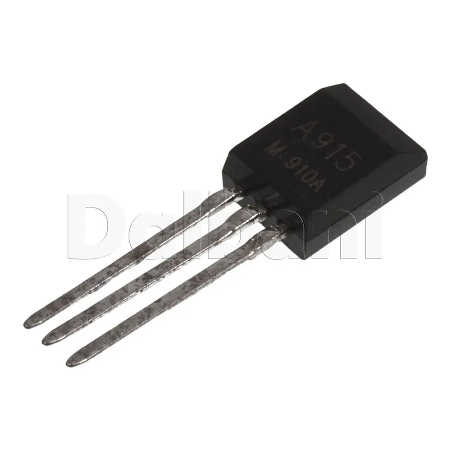
While the 2N3904 is a widely used NPN BJT, several alternatives can be used in similar applications. This section explores some common substitutes, highlighting their key differences and suitability for different scenarios. Understanding these alternatives is crucial when the 2N3904 is unavailable or when specific performance characteristics are needed.
| Transistor Model | Type | Polarity | Max Collector Current (Ic) | Typical Application | Advantages | Disadvantages |
|---|---|---|---|---|---|---|
| 2N3904 | BJT | NPN | 200mA | General purpose switching/amplification | Common and inexpensive | Lower current gain |
| 2N2222A | BJT | NPN | 800mA | Higher current switching | Higher current rating, Higher current gain | May be slightly more expensive |
| BC547 | BJT | NPN | 100mA | Low-noise amplification | Low noise, good hFE | Lower current rating than 2N3904 |
| BC537 | BJT | NPN | 100mA | Medium power switching | Medium power, good hFE | Lower current rating than 2N3904 |
| BC538 | BJT | PNP | 100mA | Medium power switching | PNP complement to BC537 | PNP polarity, not a direct substitute in all cases. |
| 2N4401 | BJT | NPN | 600mA | Medium current switching | Higher current rating | May have lower gain than 2N3904 in certain conditions |
The 2N2222A is a close alternative with a higher current rating making it suitable for higher power applications. The BC547, BC537 and 2N4401 are other NPN options with different current and gain characteristics for specific circuit needs. Additionally, consider the BC538 as a PNP transistor. When selecting an alternative, it's important to review the datasheets and ensure that the selected component meets the electrical and thermal requirements of the application.
This section addresses common questions about the 2N3904 transistor, providing clear and concise answers to help users understand its applications, characteristics, and potential alternatives. We aim to clarify any confusion and equip you with the essential knowledge for working with this ubiquitous component.
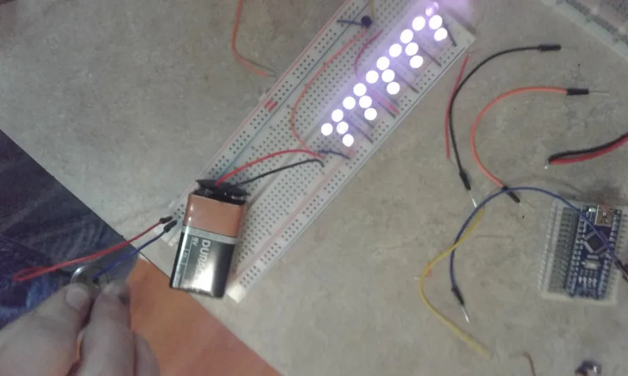
Successfully utilizing the 2N3904 transistor requires a practical understanding of its handling and testing. This section provides actionable advice to ensure your circuits function as expected, covering safe handling practices, common pitfalls to avoid, and methods to verify transistor functionality, including how to measure its current gain (hFE).
Selecting the appropriate transistor for a given application hinges on understanding its key specifications and how these compare to those of other common transistors. This section provides a detailed comparison of the 2N3904 with several widely used alternatives, including the 2N3906, 2N2222, and BC547, to facilitate informed decision-making in circuit design.
| Parameter | 2N3904 (NPN) | 2N3906 (PNP) | 2N2222 (NPN) | BC547 (NPN) |
|---|---|---|---|---|
| Polarity | NPN | PNP | NPN | NPN |
| Maximum Collector Current (Ic) | 200 mA | 200 mA | 800 mA | 100 mA |
| Maximum Collector-Emitter Voltage (Vceo) | 40 V | 40 V | 40 V | 45 V |
| Maximum Power Dissipation (Pd) | 625 mW | 625 mW | 800 mW | 500 mW |
| Typical Current Gain (hFE) | 100-300 | 100-300 | 35-300 | 110-800 |
| Transition Frequency (ft) | 300 MHz | 250 MHz | 300 MHz | 300 MHz |
| Package | TO-92 | TO-92 | TO-92 | TO-92 |
The 2N3904 transistor, a fundamental building block in electronics, serves as a reliable NPN component for switching and amplification. By understanding its basic structure, pin configurations, and applications, you're better equipped to integrate the 2N3904 or its alternatives into various circuits. Whether you are building a simple light switch or a complex signal amplifier, the principles learned here will be foundational, enabling your innovative designs to power real-world applications and further innovation within the electronics realm. The 2N3904, though small, holds significant power in the world of electronics.

