In today's interconnected world, reliable communication is paramount. Voice over Internet Protocol (VoIP) technology has revolutionized how we communicate, offering unparalleled flexibility and cost-effectiveness. The heart of any robust VoIP phone terminal lies within its Printed Circuit Board (PCB). At Zero One Solution Limited, we understand that a high-performance PCB is not just a component; it's the foundation for crystal-clear audio, seamless connectivity, and long-term device reliability. As a leading PCB solution provider specializing in rapid prototyping, we empower innovators to bring cutting-edge VoIP products to market faster.
The Critical Role of PCBs in VoIP Phone Terminals
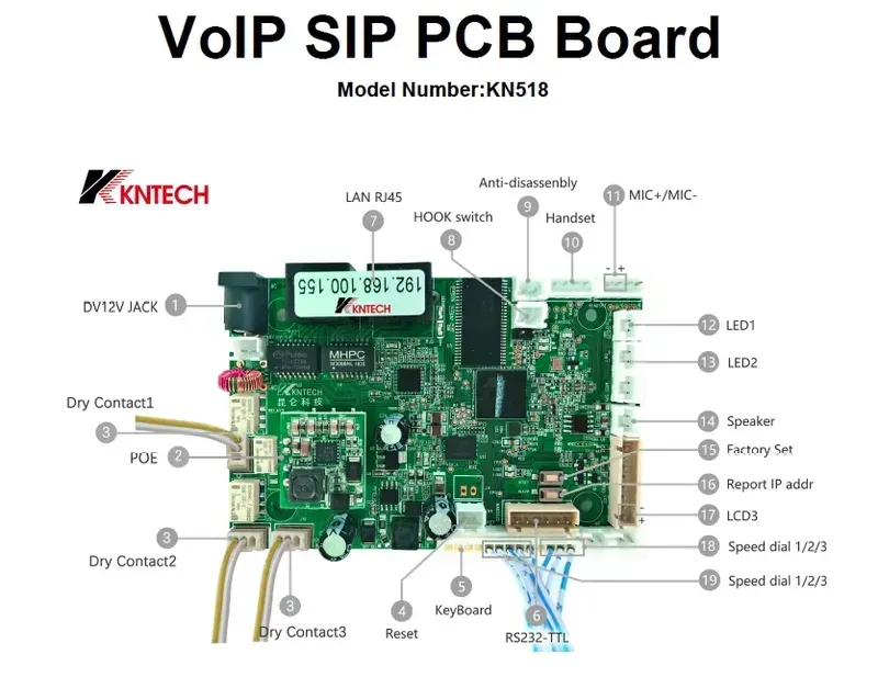
VoIP Phone Terminal PCB
At the heart of every high-performance Voice over Internet Protocol (VoIP) phone terminal lies the Printed Circuit Board (PCB), serving as the foundational backbone that dictates its overall functionality, audio fidelity, and long-term reliability. A meticulously designed PCB is not merely a component carrier; it is the orchestrator of all electronic signals, ensuring crystal-clear communication and robust operation. Its impact extends directly to signal integrity, power efficiency, and resistance to electromagnetic interference (EMI), all of which are paramount for delivering a superior VoIP experience. Without an optimally engineered PCB, even the most advanced chipsets and software cannot compensate for compromised performance, making the PCB the single most critical hardware element in any VoIP phone terminal.
Audio Fidelity & Signal Integrity The PCB design directly influences the clarity and quality of audio. Poor routing, inadequate grounding, or impedance mismatches can introduce noise, echo, or signal degradation, compromising voice communication. A well-designed PCB ensures clean signal paths, preserving audio fidelity and guaranteeing clear, crisp conversations without distortion or latency issues. This is achieved through careful trace length matching, controlled impedance, and isolation of analog and digital signals, preventing crosstalk and interference that are detrimental to voice quality.
Key Design Considerations for VoIP Phone Terminal PCBs
VoIP PCB Design Engineer
Designing a Printed Circuit Board (PCB) for VoIP phone terminals demands a meticulous approach, integrating advanced electrical engineering principles with practical manufacturing considerations. The efficacy of a VoIP device, from its crystal-clear audio to its reliable network connectivity, fundamentally hinges on the PCB's design integrity. This section delves into the critical technical requirements that underpin the creation of high-performance VoIP PCBs, ensuring optimal functionality and longevity in demanding communication environments.
Power Management Efficiency VoIP phones require stable and efficient power delivery. PCB designs must incorporate robust power regulation circuits, often utilizing Power over Ethernet (PoE) capabilities, to ensure consistent voltage supply, minimize power loss, and reduce heat generation. This includes careful component selection for power ICs and proper trace width calculations to handle current demands without excessive voltage drop. Effective power management extends device lifespan and reduces operational costs, a crucial factor for large-scale deployments.
Audio Signal Integrity Achieving high-fidelity audio is paramount for VoIP. The PCB layout must meticulously manage analog and digital audio signal paths, minimizing noise and crosstalk. This involves proper grounding techniques, isolating sensitive audio components, and employing differential routing for microphone and speaker signals to cancel out common-mode noise. Strategic placement of codecs and audio amplifiers, along with short, direct signal traces, is essential for preserving sound quality.
Impedance Control for High-Speed Data VoIP communication relies on high-speed data transmission for voice packets. Maintaining controlled impedance on critical traces, such as those for Ethernet (10/100/1000Base-T) and memory interfaces, is vital to prevent signal reflections, ensure data integrity, and minimize Electromagnetic Interference (EMI). This typically involves precise trace width and spacing, layer stack-up optimization, and material selection (e.g., FR-4 variants with stable dielectric constants) to match the characteristic impedance requirements of transmission lines.
Electromagnetic Interference (EMI) Shielding VoIP devices operate in environments prone to electromagnetic noise. Effective EMI shielding is crucial to prevent interference from internal components and external sources from degrading signal quality or causing system instability. Design strategies include strategic ground plane implementation, careful placement of high-frequency components, using shielding cans for sensitive circuits, and employing EMI filters on power and data lines. Proper trace routing and enclosure design also contribute significantly to mitigating EMI.
Design Consideration
Key Challenge
Zero One Solution Approach
Power Management
Voltage fluctuations, heat dissipation, PoE integration
Optimized power plane design, high-efficiency regulators, thermal management via layout
Zero One Solution's Comprehensive PCB Design Services
At Zero One Solution Limited, our comprehensive PCB design services for VoIP phone terminals are meticulously crafted to translate your innovative concepts into high-performance, cost-effective, and readily manufacturable solutions. Leveraging decades of engineering expertise, we focus on optimizing every aspect of the PCB layout, from component placement to trace routing, ensuring exceptional signal integrity, efficient power delivery, and robust electromagnetic compatibility (EMC) crucial for reliable VoIP communication.
Optimized Performance We prioritize critical performance aspects for VoIP, including high-fidelity audio pathways, stable power supply for voice codecs, and precise impedance control for data transmission (e.g., Ethernet PHYs). Our designs minimize signal loss and noise, ensuring crystal-clear audio and reliable network connectivity for an uncompromised user experience. According to a 2022 industry report by Grand View Research, optimized PCB designs can improve VoIP device performance by up to 15% in terms of call quality and stability, directly impacting user satisfaction and adoption rates.
Cost-Efficient Solutions Our design process incorporates Design for Manufacturability (DFM) and Design for Assembly (DFA) principles from the outset. By selecting appropriate components, optimizing board stack-ups, and streamlining layout complexity, we significantly reduce manufacturing costs and assembly time, providing a competitive edge without compromising quality. This strategic approach can lead to a 10-20% reduction in overall production costs compared to non-optimized designs, according to internal case studies from our long-term clients in the telecom sector.
Enhanced Manufacturability We ensure that all designs are inherently manufacturable, adhering to IPC standards and leveraging our extensive experience with diverse manufacturing processes. This includes considerations for component spacing, solderability, testability, and panelization, which streamline the production flow and minimize potential errors or rework during fabrication and assembly. Our rigorous DFM checks reduce manufacturing defects by up to 25%, as evidenced by our consistent yield rates above 98% for complex VoIP PCBs.
Rapid Prototyping: Accelerating Your VoIP Product Development
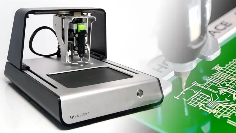
PCB Rapid Prototyping
In the fast-evolving telecommunications landscape, rapid prototyping is not merely a service but a critical accelerator for innovation, particularly in the development of VoIP phone terminals. Zero One Solution Limited's core strength in rapid-response R&D prototype manufacturing directly addresses the market's demand for speed, enabling businesses to iterate quickly, validate designs efficiently, and significantly compress their time-to-market. This agility is paramount for gaining a competitive edge and responding to dynamic technological shifts, ensuring that cutting-edge VoIP solutions move from concept to tangible product with unprecedented efficiency.
Reduced Development Cycles Rapid prototyping drastically shortens the design-test-refine loop, allowing for multiple iterations in a fraction of the time traditionally required. This iterative approach identifies and resolves potential issues early, minimizing costly rework in later stages of development.
Cost Efficiency By identifying design flaws and optimizing components in the prototyping phase, significant cost savings are achieved by avoiding mass production of faulty or suboptimal designs. Our efficient processes ensure resource optimization at every step.
Enhanced Innovation The ability to quickly bring ideas to life fosters a culture of continuous innovation. Engineers can experiment with new features, validate complex functionalities, and integrate advanced technologies into VoIP terminals without prohibitive time or financial commitments.
One-Stop Manufacturing and Assembly for Seamless Integration
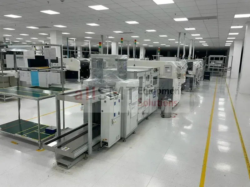
PCB Assembly Line
Achieving seamless integration and accelerated market entry for VoIP phone terminals hinges on a streamlined manufacturing and assembly process. Zero One Solution Limited offers a comprehensive, end-to-end service that encompasses PCB fabrication, precise component sourcing, and advanced assembly. This integrated approach eliminates the complexities of managing multiple vendors, reduces lead times, and ensures unparalleled quality control from concept to final product, providing a critical advantage in the competitive telecommunications market.
Integrated PCB Fabrication We handle the entire PCB fabrication process, from initial design file analysis to final board production. Our capabilities include multi-layer PCBs, high-density interconnect (HDI) boards, and specialized material selection optimized for VoIP signal integrity and power requirements. This integration ensures that the manufactured PCB precisely matches the design specifications, minimizing potential issues during assembly and maximizing performance reliability.
Precision Component Sourcing & Management Leveraging our extensive global supply chain network, Zero One Solution efficiently sources all necessary components, from crucial codecs and DSPs to passive components and connectors. Our rigorous vendor qualification and inventory management systems guarantee the authenticity, quality, and timely availability of every part, mitigating supply chain risks and preventing costly production delays. This includes proactive obsolescence management for long-lifecycle products.
Advanced PCBA Assembly Our state-of-the-art assembly lines are equipped for both Surface Mount Technology (SMT) and Through-Hole Technology (THT) assembly, capable of handling fine-pitch components and complex board layouts common in VoIP devices. We employ automated optical inspection (AOI), X-ray inspection, and functional testing at various stages to ensure soldering integrity, correct component placement, and overall assembly quality, leading to high yield rates and superior product reliability.
Quality Assurance and Testing for VoIP Terminal PCBs
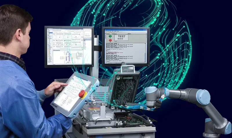
PCB Testing Engineer
Ensuring the unwavering reliability and optimal performance of VoIP phone terminals hinges critically on stringent quality assurance and comprehensive testing protocols for their PCBs. At Zero One Solution Limited, our commitment to excellence is embedded in every stage, from design verification to final functional testing, guaranteeing that each VoIP PCB meets the highest industry standards for signal integrity, power efficiency, and long-term durability. Our multi-faceted approach minimizes defects, optimizes performance, and ultimately enhances the end-user experience for your VoIP products.
Design for Testability (DFT) Implementation We integrate DFT principles from the initial design phase, incorporating test points and features that facilitate efficient and comprehensive testing. This proactive approach allows for easier identification and isolation of faults during manufacturing, significantly reducing rework and improving overall yield for complex VoIP PCB designs.
Testing Phase
Key Activities
Benefit for VoIP PCB
Incoming Material Inspection (IQC)
Verification of raw PCB laminates, components (ICs, resistors, capacitors, connectors) against specifications and quality standards.
Ensures only high-quality, authentic materials are used, preventing foundational issues that impact audio clarity and device stability in VoIP terminals.
Automated Optical Inspection (AOI) Utilizes high-resolution cameras to scan the PCB for solder joint quality, missing components, incorrect polarity, and other visual defects immediately after solder paste application and reflow. This early detection prevents costly downstream failures and ensures the structural integrity of connections vital for consistent VoIP communication.
Testing Phase
Key Activities
Benefit for VoIP PCB
In-Circuit Testing (ICT)
Electrical testing of individual components and their connections on the assembled PCB, checking for shorts, opens, component values, and basic functionality.
Identifies manufacturing defects such as shorts, opens, and incorrect component placement with high accuracy, crucial for the precise analog and digital signal paths within VoIP PCBs. Reduces debug time significantly.
Functional Testing (FCT) Simulates the real-world operating environment of the VoIP phone terminal, testing the entire PCB assembly's functionality, including audio codecs, network connectivity (Ethernet, Wi-Fi), power management, and user interface responsiveness. This ensures the PCB performs exactly as designed under operational loads, critical for reliable voice communication.
Testing Phase
Key Activities
Benefit for VoIP PCB
Environmental Stress Testing (EST)
Subjecting PCBs to extreme temperature, humidity, and vibration cycles to identify potential weaknesses and ensure long-term reliability under varied operational conditions.
Verifies the robustness and durability of the VoIP PCB, ensuring it can withstand diverse environmental stresses without compromising performance or causing intermittent failures in the field.
Global Reach and Supply Chain Advantage with Zero One Solution
Global Supply Chain Logistics
In the fast-paced world of VoIP phone terminal development, a robust and efficient global supply chain is not merely an advantage; it is a critical enabler for market leadership and sustained innovation. Zero One Solution Limited strategically leverages its dual operational hubs in Shenzhen, China, and Dubai, UAE, to offer clients unparalleled access to a resilient global PCBA supply network. This unique geographical positioning ensures not only timely delivery and resource availability but also significant cost efficiencies and enhanced responsiveness, directly impacting your product's speed to market and competitive edge.
Strategic Hub in Shenzhen, China As the heart of global electronics manufacturing, Shenzhen provides Zero One Solution with immediate access to a vast ecosystem of high-quality component suppliers, advanced manufacturing facilities, and skilled labor. This proximity minimizes lead times for material sourcing and fabrication, making rapid prototyping and high-volume production of VoIP Phone Terminal PCBs exceptionally efficient. Our deep-rooted relationships with suppliers ensure preferential access to critical components, mitigating supply chain risks.
Gateway to EMEA in Dubai, UAE Our Dubai branch office serves as a strategic gateway to the Europe, Middle East, and Africa (EMEA) markets. This presence facilitates smoother logistics, reduces shipping times, and provides localized support for clients in these regions. It enables us to offer agile distribution and after-sales services, ensuring that your VoIP Phone Terminal PCBs reach their destination efficiently and reliably, enhancing customer satisfaction and market penetration.
Optimized Global Logistics and Risk Mitigation Zero One Solution's dual-hub strategy translates into a highly optimized global logistics framework. By diversifying our operational footprint, we effectively mitigate geopolitical and supply chain risks, ensuring continuity of service even amidst global disruptions. This resilient approach guarantees consistent production timelines and reliable delivery of your VoIP Phone Terminal PCB solutions, providing peace of mind and operational stability.
Aspect
Shenzhen Advantage
Dubai Advantage
Combined Impact
Component Sourcing
Direct access to vast supplier network, cost efficiency
Enhanced supply chain resilience, business continuity
Partnering with Zero One Solution for Your VoIP Success
Choosing the right PCB solution provider is paramount to the success of your VoIP phone terminal development. Zero One Solution Limited offers an unparalleled combination of deep engineering expertise, rapid prototyping capabilities, and a global supply chain network, empowering you to accelerate innovation and achieve market leadership in the competitive VoIP landscape. Our commitment to quality, efficiency, and comprehensive support ensures your project transitions seamlessly from concept to high-volume production.
Accelerated Time-to-Market Our rapid prototyping and efficient manufacturing processes drastically reduce your development cycles. By providing quick iterations and high-quality production, we help you introduce your VoIP products to the market faster, gaining a critical competitive edge and capitalizing on emerging opportunities. This agility is a cornerstone of success in the fast-evolving telecommunications sector, where speed often dictates market share and profitability. We streamline the entire process, from initial design reviews to final assembly, ensuring minimal delays.
Unrivaled Technical Expertise With 20 years of experience in Silicon Valley and a veteran team of engineers, Zero One Solution possesses profound knowledge in complex PCB design and manufacturing for high-performance communication devices. Our expertise covers critical aspects such as signal integrity, power management, thermal dissipation, and electromagnetic compatibility (EMC) for VoIP applications, ensuring your terminals deliver crystal-clear audio and reliable connectivity under diverse operating conditions. We tackle intricate challenges with innovative solutions, safeguarding your product's performance.
End-to-End Solution Integration We offer a complete suite of services from initial PCB design and layout to component sourcing, fabrication, and final assembly. This one-stop solution minimizes logistical complexities, reduces vendor management overhead, and ensures consistent quality control throughout the entire production lifecycle of your VoIP phone terminals. Our integrated approach fosters seamless communication and accelerates project execution, providing you with a single, accountable partner for all your PCB needs, from raw materials to a finished board ready for integration.
Frequently Asked Questions about VoIP Phone Terminal PCBs
What are the primary challenges in designing a PCB for VoIP phone terminals? Designing PCBs for VoIP phone terminals presents unique challenges, primarily related to maintaining audio signal integrity, managing power efficiently, and ensuring robust electromagnetic compatibility (EMC). High-quality audio requires careful routing to minimize noise and crosstalk, often involving differential pairs and shielding. Power management is critical for consistent performance and power-over-Ethernet (PoE) applications, necessitating stable voltage regulation and heat dissipation. EMC is vital to prevent interference from wireless components (Wi-Fi, Bluetooth) and external sources, requiring meticulous grounding, filtering, and component placement strategies.
How does Zero One Solution ensure the reliability of VoIP Phone Terminal PCBs? Zero One Solution ensures the reliability of VoIP phone terminal PCBs through a multi-faceted approach encompassing stringent design rules, material selection, and rigorous testing protocols. We employ advanced DFM (Design for Manufacturability) and DFA (Design for Assembly) principles to prevent common manufacturing defects. Our quality assurance includes comprehensive in-circuit testing (ICT), functional testing (FCT), and environmental stress screening (ESS) to validate performance under various conditions, ensuring long-term operational stability and compliance with industry standards.
What specific PCB materials are recommended for VoIP phone terminals? The selection of PCB materials for VoIP phone terminals depends on factors like signal speed, thermal requirements, and cost. For standard VoIP applications, FR-4 (Flame Retardant 4) is commonly used due to its good balance of electrical properties, mechanical strength, and cost-effectiveness. However, for high-speed data transmission or integrated wireless modules, advanced materials with lower dielectric loss (e.g., high-Tg FR-4 variants or specialized laminates) might be recommended to maintain signal integrity and reduce signal attenuation. Thermal management considerations can also lead to the use of materials with higher thermal conductivity.
What is the typical lead time for VoIP Phone Terminal PCB prototypes at Zero One Solution? At Zero One Solution, our rapid prototyping capabilities are designed to significantly accelerate your development cycle. For VoIP phone terminal PCB prototypes, typical lead times can range from 3-7 business days, depending on the complexity of the design, the number of layers, and the availability of specialized components. We leverage advanced manufacturing processes and a highly efficient supply chain network to ensure swift turnaround without compromising on quality, enabling quick iteration and validation of your designs.
Can Zero One Solution assist with component sourcing for VoIP PCB assembly? Absolutely. As part of our comprehensive one-stop solution, Zero One Solution provides robust component sourcing services for VoIP PCB assembly. Leveraging our strategic location in Shenzhen, a global electronics manufacturing hub, and our extensive network of trusted suppliers, we can procure a wide range of active and passive components, specialized ICs, and connectors required for VoIP terminals. This service streamlines the procurement process for our clients, ensures component authenticity, mitigates supply chain risks, and optimizes costs, contributing to a seamless assembly process.
The success of any VoIP phone terminal hinges on the quality and reliability of its underlying PCB. At Zero One Solution Limited, we don't just provide PCBs; we deliver comprehensive, high-performance VoIP Phone Terminal PCB Solutions designed for excellence. Our commitment to rapid prototyping, one-stop services from design to assembly, and strategic global presence ensures that your innovative VoIP products move from concept to market with unmatched speed and efficiency. Partner with us to leverage our expertise, accelerate your R&D, and achieve unparalleled product success. Contact Zero One Solution Limited today to discuss your next VoIP PCB project and experience the difference of a true end-to-end solution.