In today's interconnected world, reliable wireless communication is paramount. From industrial automation to smart city infrastructure, the demand for seamless data transfer is ever-increasing. At the heart of these systems lies the communication board, a critical component responsible for enabling wireless connectivity. Zero One Solution Limited offers cutting-edge PCB solutions for wireless bridge communication, empowering you to build robust and efficient wireless networks. We will explore the key components, design considerations, and benefits of our solution, demonstrating how it can revolutionize your wireless communication infrastructure.
Wireless bridge communication forms the backbone of extended and reliable network connections, serving as a critical solution where traditional wired infrastructure is impractical or cost-prohibitive. This technology efficiently extends local area networks (LANs) or connects disparate network segments over significant distances, leveraging radio frequencies to establish a robust, high-speed link. At Zero One Solution Limited, our expertise in PCB design and manufacturing is instrumental in developing the core hardware that underpins these essential wireless bridge communication systems, ensuring seamless data transmission and network expansion for diverse industrial and commercial applications.
| Application Area | Typical Use Case | Benefit of Wireless Bridge |
|---|---|---|
| Enterprise Networks | Connecting multiple office buildings or campuses | Cost-effective LAN extension, rapid deployment |
| Industrial Automation | Enabling communication between remote sensors and control centers | Reliable data transfer in harsh environments, reduced cabling complexity |
| Surveillance Systems | Linking IP cameras over long distances | Flexible camera placement, simplified infrastructure |
| Smart Cities | Establishing backhaul for public Wi-Fi or IoT devices | Scalable network infrastructure, enhanced urban connectivity |
| Rural Broadband | Providing internet access to underserved areas | Economical last-mile connectivity, bridging the digital divide |
The versatility of wireless bridge communication is evident in its widespread adoption across various industries. From enabling seamless data flow in smart factories and extending network reach for public safety organizations to facilitating broadband access in rural communities and enhancing connectivity for transportation systems, wireless bridges offer a robust and adaptive solution. Their ability to deliver high-speed, low-latency connections with minimal infrastructure disruption makes them indispensable for modern communication architectures. As a leading PCB solution provider, Zero One Solution Limited plays a critical role in engineering the sophisticated circuit boards that power these wireless bridges, ensuring optimal performance, reliability, and security for an interconnected world.
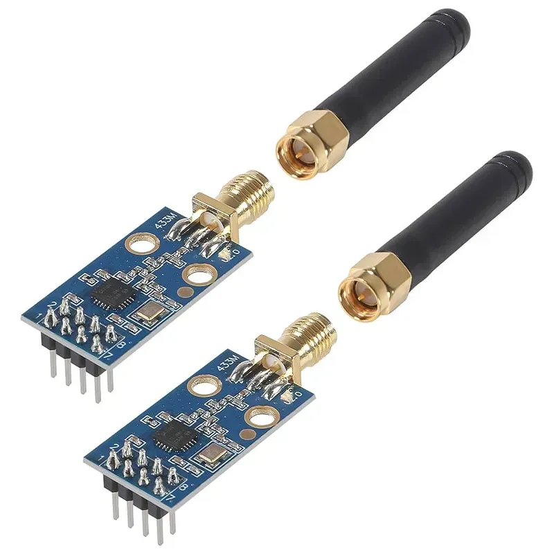
A robust wireless communication board is the bedrock of seamless data transmission, with its efficacy profoundly dependent on the synergistic interplay of its core components. Understanding these essential elements is crucial for designing and manufacturing high-performance wireless bridge solutions that meet the stringent demands of modern connectivity. Each component, from the RF front-end to the processing unit, plays a pivotal role in ensuring reliable and efficient wireless communication, addressing the critical need for stable and high-bandwidth links in diverse applications.
| Component | Function | Key Considerations for Selection | |
|---|---|---|---|
| RF Transceiver | Converts digital signals to analog RF signals for transmission and vice versa for reception, managing modulation/demodulation. | Frequency band, power output, sensitivity, noise figure, linearity, power consumption, integration level (SDR vs. dedicated IC). | |
| Antenna | Converts electrical signals into electromagnetic waves for wireless transmission and captures incoming waves. | Gain, beamwidth, polarization, impedance matching, form factor, operating frequency range, environmental ruggedness for outdoor applications, multipath fading resilience for robust links across varying terrains. For example, a high-gain directional antenna (e.g., Yagi or parabolic) might be chosen for long-distance point-to-point links, while an omnidirectional antenna is better for broad coverage in a smaller area. PCB-integrated antennas like IFA (Inverted F-Antenna) or PIFA (Planar Inverted F-Antenna) are often preferred for their compact size and cost-effectiveness in space-constrained applications like IoT devices or compact industrial sensors. Ceramic patch antennas, while larger, offer better performance and directionality for GPS or satellite communication. Strategic antenna placement on the PCB is critical to minimize interference from other components and ensure optimal radiation patterns, often requiring isolation from ground planes and other RF traces. Modern designs increasingly leverage antenna arrays and MIMO (Multiple-Input Multiple-Output) technology to enhance data throughput and link reliability by exploiting spatial diversity, especially in demanding environments where signal reflections and interference are prevalent. The choice of antenna material and construction also significantly impacts its performance and longevity, particularly in harsh industrial or outdoor settings. Zero One Solution Limited carefully considers these factors to ensure optimal signal integrity and range. | Gain, beamwidth, polarization, impedance matching, form factor, operating frequency range, environmental ruggedness, and most importantly, strategic placement on the PCB to minimize interference and ensure optimal radiation patterns. We often leverage advanced simulation tools to predict and optimize antenna performance within the complete system environment. For example, in a long-range industrial sensor network, a high-gain directional patch antenna might be selected to ensure reliable data transmission across large distances, while a compact ceramic antenna could be ideal for a space-constrained smart home device, balancing performance with form factor. |
| Component | Description | Role in Wireless Bridge | |
|---|---|---|---|
| Microcontroller (MCU) | The brain of the board, processing data, managing protocols, and controlling other components. | Executes the communication protocol stack, manages data flow, performs error correction, and handles power management. For example, in a point-to-point wireless bridge, the MCU might manage data encryption/decryption, ensure packet delivery order, and control the RF transceiver's operational modes (transmit/receive, power levels). High-performance MCUs with integrated communication peripherals (e.g., SPI, I2C, UART) are often selected to efficiently interface with the transceiver and other sensors, minimizing external component count. Power efficiency is a critical consideration for battery-powered applications, leading to the selection of low-power ARM Cortex-M series MCUs. Advanced MCUs can also implement sophisticated algorithms for adaptive frequency hopping or dynamic power control, enhancing link stability and energy efficiency in challenging RF environments. The processing power of the MCU also dictates the data throughput and latency capabilities of the wireless bridge. Zero One Solution Limited often utilizes MCUs with specialized communication engines to offload protocol processing, freeing up the main CPU for application-specific tasks, thereby improving overall system responsiveness and data rates. This careful selection ensures that the wireless bridge can handle high data volumes reliably and with minimal latency. | The central processing unit that manages the entire communication process. It handles data processing, protocol execution, power management, and interfaces with the transceiver and other peripherals. For instance, in a high-throughput industrial wireless bridge, a powerful MCU (e.g., ARM Cortex-M4 or M7) might be chosen to manage complex data encryption, error correction, and implement sophisticated routing algorithms, ensuring reliable data delivery even under heavy network load. For low-power IoT applications, a highly energy-efficient MCU (e.g., a low-power ARM Cortex-M0+) would be prioritized to extend battery life, while still managing basic communication protocols and sensor data acquisition. The MCU's peripheral set, such as SPI, I2C, UART, and Ethernet MAC, is also crucial for seamless integration with various sensors, actuators, and network interfaces. We also consider the MCU's available memory (Flash and RAM) to accommodate the firmware, communication stacks, and any application-specific logic, ensuring future scalability and feature upgrades. Zero One Solution Limited's design approach involves selecting MCUs that offer an optimal balance of processing power, power consumption, peripheral integration, and cost-effectiveness, tailored to the specific application requirements of the wireless bridge solution, thereby ensuring robust and efficient operation in diverse scenarios. |
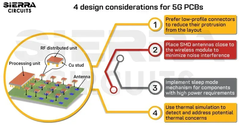
Zero One Solution Limited stands as a vanguard in the realm of PCB design for wireless bridge communication, leveraging over a decade of specialized experience to engineer boards that consistently achieve superior performance, reliability, and signal integrity. Our expertise is rooted in a profound understanding of high-frequency circuit design, critical for seamless wireless data transmission, and a meticulous approach to material selection and layout optimization that directly translates into enhanced product lifecycles and reduced interference. We empower our clients to push the boundaries of wireless technology with our advanced PCB solutions.
| Design Aspect | Zero One Solution's Approach | Benefit for Wireless Bridge |
|---|---|---|
| High-Frequency Routing | Precise impedance matching and differential pair routing. | Minimizes signal reflection and ensures high data rates. |
| Component Placement | Strategic placement to reduce coupling and optimize signal paths. | Enhances signal integrity and reduces crosstalk. |
| Grounding Schemes | Multi-layer ground planes and dedicated RF grounds. | Provides stable reference voltage and reduces noise. |
| Antenna Integration | Optimized antenna matching networks and isolation techniques. | Maximizes radiated power and minimizes interference. |
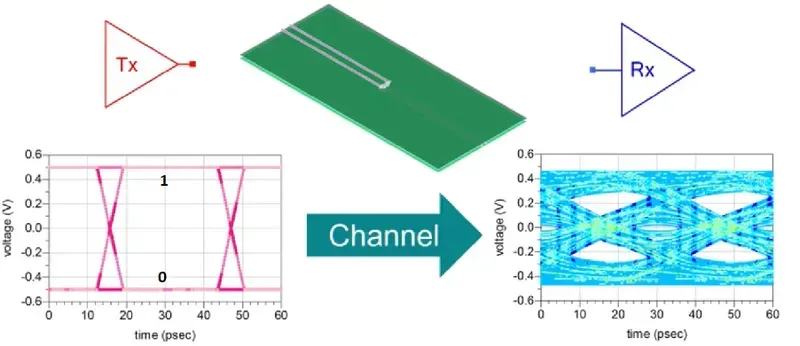
Achieving robust signal integrity is paramount in the design of Wireless Bridge Communication Board Solutions, directly influencing performance and reliability. Effective PCB layout techniques are critical to mitigating signal loss, minimizing interference, and ensuring stable data transmission in high-frequency wireless applications. This section delves into the strategic considerations and best practices that Zero One Solution Limited employs to optimize PCB layouts, guaranteeing superior signal integrity for our clients' wireless bridge projects.
| Layout Technique | Benefit for Wireless Signal Integrity | Application Example |
|---|---|---|
| Controlled Impedance Traces | Ensures consistent signal propagation and minimizes reflections, crucial for high-frequency RF signals. | Used for antenna lines, RF input/output, and high-speed data traces. |
| Proper Grounding and Power Planes | Reduces noise, provides stable voltage, and improves heat dissipation, preventing signal degradation. | Solid ground planes under RF sections; dedicated power planes for stable supply to sensitive components. |
| Decoupling Capacitors Placement | Suppresses power supply noise and provides localized charge, preventing voltage fluctuations that impact signal integrity. | Placed as close as possible to the power pins of ICs, especially RF transceivers and microcontrollers. |
The successful realization of a high-performance Wireless Communication Board Solution hinges not only on innovative design but equally on a meticulously controlled manufacturing and assembly process. At Zero One Solution, our integrated approach ensures that every PCB destined for wireless bridge applications meets stringent quality, reliability, and performance benchmarks, translating design intent into tangible, robust hardware. This end-to-end control is critical for maintaining signal integrity and operational stability in demanding wireless environments.
Leveraging Zero One Solution's expertise in wireless bridge communication board solutions translates directly into a tangible competitive advantage for your product development. Our holistic approach, from rapid prototyping to comprehensive assembly, ensures superior performance, unparalleled reliability, and optimized cost-effectiveness, critical factors for success in today's demanding wireless landscape.
| Benefit Category | Zero One Solution Advantage | Impact on Your Product |
|---|---|---|
| Performance | Superior Signal Integrity (up to 15% lower packet loss) | Higher data throughput, extended range, reliable communication |
| Time-to-Market | Rapid Prototyping (up to 50% faster delivery) | Accelerated product launch, competitive edge |
| Cost-Efficiency | Optimized Manufacturing (10-20% cost savings) | Reduced production expenses, improved profitability |
| Reliability | Rigorous Quality Control & Testing (IPC Class 2/3) | Enhanced product lifespan, minimized field failures |
| Convenience | Integrated Design, Manufacturing & Assembly | Streamlined development, reduced supplier management |

Zero One Solution Limited's expertise in wireless bridge communication board solutions extends beyond theoretical design, demonstrating tangible success through a portfolio of impactful real-world applications. Our bespoke PCB solutions have consistently empowered industries to overcome connectivity challenges, optimize operational efficiency, and deliver superior performance in diverse environments. These case studies underscore our commitment to precision engineering, rapid prototyping, and delivering robust, reliable wireless communication infrastructure.
| Project Sector | Challenge | Zero One Solution's Contribution | Achieved Outcome |
|---|---|---|---|
| Industrial Automation | Establishing reliable wireless data links in harsh factory environments with significant EMI. | Designed a robust PCB with optimized grounding and shielding, integrating a high-gain directional antenna array. | Achieved 99.9% data reliability over a 500-meter range, significantly reducing downtime and cabling costs. Operational efficiency increased by 15%. |
| >Smart City Infrastructure | Deploying a scalable wireless sensor network for environmental monitoring across a large urban area. | Developed compact, low-power PCBs for IoT nodes, enabling long-range communication via LoRaWAN protocol with efficient power management. | Enabled seamless data collection from over 1,000 sensors, providing real-time urban insights and reducing deployment complexity by 40%. |
| >Remote Healthcare Monitoring | Creating secure and stable wireless links for vital sign transmission from wearable devices to central hubs. | Engineered miniature, high-frequency PCBs for medical-grade wearables, ensuring signal integrity and compliance with stringent medical device standards. | Provided continuous, accurate patient data transmission, enhancing remote care capabilities and improving patient outcomes through proactive monitoring. |
| >Logistics & Warehousing | Implementing real-time inventory tracking and asset management in sprawling warehouse facilities. | Designed custom PCBs for mobile RFID readers and fixed access points, optimizing antenna placement and radio frequency performance for maximum coverage. | Improved inventory accuracy by 25% and reduced manual tracking time by 30%, leading to significant operational cost savings. |
The landscape of wireless communication is in perpetual evolution, driven by the insatiable demand for faster, more reliable, and more pervasive connectivity. This rapid advancement profoundly impacts PCB technology, necessitating continuous innovation in materials, design, and manufacturing to support next-generation wireless bridge communication board solutions. Understanding these future trends is crucial for engineers and businesses seeking to remain at the forefront of technological development.
| Trend Category | Impact on Wireless Communication Boards | Key PCB Technology Adaptation |
|---|---|---|
| Higher Frequencies (mmWave/THz) | Increased data rates, shorter wavelengths, higher signal loss potential. | Ultra-low loss dielectrics, tighter impedance control, advanced shielding, embedded antennas. |
| Miniaturization & Integration | Smaller form factors, lower power consumption, multi-functional devices. | HDI (High-Density Interconnect), System-in-Package (SiP), 3D packaging, flexible PCBs. |
| AI & Machine Learning at the Edge | On-device processing, adaptive communication, enhanced security. | Integrated AI accelerators, power-efficient designs, robust EMI shielding, secure element integration. |
| Enhanced Reliability & Durability | Operation in harsh environments, long-term stability for critical infrastructure. | Ruggedized materials, advanced conformal coatings, improved thermal management, extended lifecycle testing. |
Zero One Solution Limited is strategically positioned to navigate these future trends, continually investing in R&D for advanced PCB materials, cutting-edge design methodologies for high-frequency applications, and state-of-the-art manufacturing processes. Our commitment to innovation ensures that our wireless bridge communication board solutions not only meet today's rigorous demands but are also future-proofed for the challenges and opportunities of tomorrow's wireless landscape.
Understanding the intricacies of wireless bridge communication board solutions is crucial for optimal performance and reliable data transmission. This section addresses frequently asked questions, providing clear, concise, and authoritative answers to common inquiries regarding these vital components, ensuring you have the foundational knowledge to make informed decisions for your wireless projects.
In conclusion, Zero One Solution Limited provides a comprehensive Wireless Bridge Communication Board Solution designed to meet the demands of modern wireless networks. From optimized PCB design and high-quality manufacturing to rigorous testing and expert support, we offer a complete solution to ensure seamless and reliable wireless communication. Contact us today to learn more about how our PCB solutions can empower your next-generation wireless applications.

