In today's rapidly evolving technological landscape, wireless transmission modules are at the heart of countless innovations, from IoT devices to sophisticated communication systems. The PCB (Printed Circuit Board) forms the backbone of these modules, and its design and execution are critical for achieving optimal performance, reliability, and efficiency. Zero One Solution Limited specializes in providing comprehensive PCB solutions tailored for wireless transmission modules, empowering our clients to push the boundaries of what's possible. This article will delve into the intricacies of wireless transmission module PCB solutions, exploring key considerations, design best practices, and the expertise that Zero One Solution brings to the table. Whether you're developing a cutting-edge IoT device or refining a complex communication system, understanding the nuances of PCB design is paramount to your success.
Introduction to Wireless Transmission Module PCBs
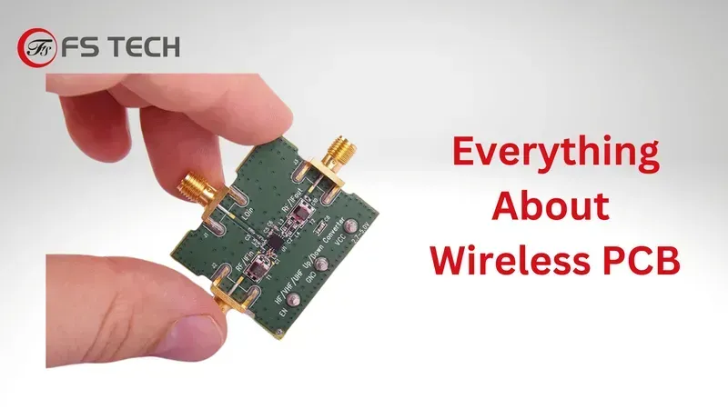
Wireless Transmission Module PCBs are the foundational hardware enabling seamless wireless communication across diverse applications, from IoT devices to sophisticated telecommunications systems. These specialized Printed Circuit Boards are meticulously engineered to handle high-frequency signals with exceptional integrity, serving as the critical backbone for efficient data transmission and reception without physical connections. Their design and manufacturing demand precision to ensure optimal performance, minimal signal loss, and reliable operation in an increasingly connected world, ultimately transforming complex wireless protocols into tangible, functional circuits.
What is the primary function of a PCB in a wireless transmission module? The primary function of a PCB in a wireless transmission module is to provide a stable and optimized platform for mounting and interconnecting electronic components, facilitating the efficient transmission and reception of radio frequency (RF) signals. It manages signal routing, impedance control, power distribution, and thermal dissipation, all crucial for maintaining signal integrity and module performance. Without a precisely designed PCB, the delicate high-frequency signals would suffer from significant losses, interference, and impedance mismatches, rendering the module ineffective for reliable wireless communication.
Key Feature
Impact on Wireless Performance
High-Frequency Material
Minimizes dielectric loss and signal attenuation at high frequencies, crucial for maintaining signal strength over distances and reducing power consumption in wireless modules (e.g., Rogers, Arlon materials).
Controlled Impedance Traces
Ensures consistent impedance matching across the transmission lines, preventing signal reflections and maximizing power transfer efficiency for clear, reliable wireless communication. Typically 50-ohm for RF traces, verified through TDR measurements and precise trace geometry calculations (width, dielectric constant, copper thickness).
Ground Plane Management
Provides a stable reference voltage, reduces noise, and improves EMI shielding by isolating sensitive RF circuits, critical for preventing interference in wireless applications. Multi-layer boards with dedicated ground planes are standard for robust RF performance, often employing stitching vias to connect ground planes across layers for enhanced performance and thermal dissipation.
The design of Wireless Transmission Module PCBs presents unique challenges due to the high-frequency nature of RF signals. Unlike standard digital PCBs, wireless PCBs require stringent attention to factors such as signal integrity, impedance control, electromagnetic interference (EMI) shielding, and thermal management. Material selection is paramount, with specialized high-frequency laminates like Rogers or Arlon often preferred over FR-4 for their lower dielectric loss and stable dielectric constant across varying frequencies and temperatures. Careful trace routing, optimal ground plane implementation, and precise component placement are essential to minimize signal degradation, prevent reflections, and ensure the module operates within its specified performance parameters. These detailed considerations are what transform a basic circuit board into a high-performance wireless enabler.
Key Considerations in Wireless PCB Design
Designing Printed Circuit Boards (PCBs) for wireless transmission modules presents unique challenges that demand meticulous attention to various critical factors. Unlike conventional PCB designs, wireless applications operate at high frequencies, where even minor discrepancies can significantly impact performance, signal integrity, and overall device reliability. A deep understanding and precise implementation of these considerations are paramount to ensuring that wireless communication is efficient, stable, and compliant with regulatory standards.
Frequency and Wavelength Management Wireless signals operate at specific frequencies, and the physical dimensions on the PCB, such as trace lengths, must be designed with respect to the signal's wavelength. Improper length matching or abrupt changes in trace geometry can lead to signal reflections and power loss. Designers must accurately calculate wavelengths for their operating frequencies and use tools like electromagnetic field solvers to simulate and optimize trace layouts.
Impedance Control and Matching Maintaining a consistent impedance throughout the signal path is fundamental for high-frequency designs. Any impedance mismatch can cause signal reflections, leading to standing waves, increased noise, and reduced power transfer efficiency. This is particularly crucial for RF traces, antenna feeds, and high-speed data lines. Careful selection of dielectric materials, trace width, and copper thickness, often in conjunction with controlled impedance stack-ups, is essential to achieve the desired characteristic impedance (e.g., 50 ohms or 75 ohms).
Signal Integrity and Noise Reduction Ensuring signal integrity involves minimizing signal distortion, crosstalk, and electromagnetic interference (EMI). This requires proper grounding strategies, including solid ground planes, via stitching, and careful separation of analog and digital signals. Decoupling capacitors should be strategically placed near power pins of integrated circuits to mitigate power supply noise. Shielding techniques, such as guard rings and component enclosures, are often employed to prevent external interference and contain internal emissions.
Thermal Management High-frequency wireless modules, especially those with power amplifiers, can generate significant heat. Effective thermal management is crucial to prevent performance degradation, component damage, and reduced lifespan. This involves incorporating thermal vias, larger copper pours, and heat sinks where necessary. Simulating thermal performance during the design phase helps identify hotspots and optimize heat dissipation strategies to maintain components within their safe operating temperatures.
Component Placement and Isolation The physical arrangement of components on a wireless PCB directly influences its performance. Sensitive RF components, such as amplifiers and filters, should be placed strategically to minimize coupling and interference. High-speed digital circuits should be separated from analog and RF sections. Shielding between different functional blocks, either through physical barriers or ground planes, is often necessary to achieve optimal isolation and prevent unwanted interactions.
The selection of appropriate PCB materials is paramount for the optimal performance of wireless transmission modules, directly impacting signal integrity and minimizing power loss at high frequencies. High-frequency applications, typical of wireless communication, demand substrates with specific dielectric properties and low dissipation factors to ensure reliable and efficient signal propagation. Choosing the right material can significantly reduce insertion loss, enhance impedance control, and improve the overall efficiency and range of wireless devices.
Material Type
Key Characteristics
Typical Applications
Advantages
Disadvantages
FR-4
Standard epoxy laminate; Tg ~135-180°C
Low-frequency digital, power supplies
Cost-effective, widely available
High Df and Dk variations at high frequencies
Rogers (PTFE-based)
Low Df and Dk, stable over frequency, excellent thermal stability
RF/Microwave, antennas, high-speed digital
Low signal loss, superior impedance control
Higher cost, specialized processing
Nelco (Hydrocarbon Ceramic)
Excellent Dk stability, low Df, good thermal performance
RF power amplifiers, base stations
High reliability, consistent performance
Moderate cost, specific processing needs
Arlon (Polyimide-based)
Good thermal and chemical resistance, moderate Df/Dk
High-temperature applications, aerospace RF
Durable, good mechanical properties
Higher cost than FR-4, not as low loss as PTFE
What are the critical material properties for high-frequency PCB design? Key properties include Dielectric Constant (Dk or εr) for signal propagation speed, Dissipation Factor (Df or tan δ) for signal loss, and thermal stability (Tg, Td) to withstand manufacturing processes and operational temperatures. Lower Df values are crucial for minimizing signal attenuation at higher frequencies, while consistent Dk across the board ensures predictable impedance.
Why is FR-4 often unsuitable for high-frequency wireless applications? While cost-effective and widely used for general-purpose PCBs, FR-4's dielectric constant (Dk) and dissipation factor (Df) vary significantly with frequency and temperature. This variability leads to increased signal loss, impedance mismatches, and reduced performance in high-frequency wireless transmission modules, making it less ideal for applications above 1-2 GHz compared to specialized RF laminates.
How does material selection impact signal integrity in wireless PCBs? Material selection directly influences signal integrity by affecting signal speed, attenuation, and reflection. Low Df materials minimize energy loss as heat, preserving signal strength. Stable Dk materials ensure consistent characteristic impedance, preventing reflections that can degrade signal quality. Proper material choice is essential for maintaining signal integrity and maximizing the range and reliability of wireless communication.
What is the significance of the Dissipation Factor (Df) in high-frequency materials? The Dissipation Factor (Df), also known as loss tangent, quantifies the amount of electrical energy absorbed by the PCB material and converted into heat. For high-frequency applications, a lower Df is critical because it indicates less signal loss, allowing more of the transmitted power to reach the antenna, thus improving the efficiency and range of the wireless module. Higher Df materials lead to significant signal attenuation, especially over longer trace lengths.
RF Layout Techniques for Optimal Performance
RF PCB Layout
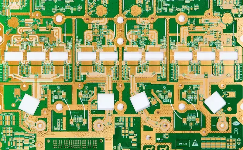
Achieving optimal performance in wireless transmission modules hinges critically on sophisticated RF layout techniques that minimize interference, reduce signal reflections, and enhance signal integrity. This precision engineering ensures that high-frequency signals traverse the PCB with minimal loss and distortion, which is paramount for reliable wireless communication. Effective RF layout is not merely about component placement but involves a deep understanding of electromagnetic principles, ensuring that the physical design supports the theoretical RF behavior.
Ground Plane Integrity A solid, uninterrupted ground plane is fundamental for RF PCBs. It provides a stable reference voltage, minimizes ground bounce, and acts as a shield against electromagnetic interference (EMI). Breaks or slots in the ground plane can create unpredictable current paths and compromise signal integrity, leading to increased noise and reflections. Multilayer PCBs often utilize dedicated ground layers to achieve superior RF performance and isolation between different signal types.
RF Layout Technique
Benefit
Common Pitfall
Controlled Impedance Traces
Ensures consistent signal transmission by matching trace impedance to the source/load.
Variations in trace width/dielectric constant causing reflections and signal loss.
Minimizing Trace Lengths
Reduces signal attenuation, parasitic capacitance, and inductance.
Excessively long traces increasing susceptibility to noise and signal degradation.
Component Placement & Isolation
Reduces crosstalk and mutual interference between sensitive RF components.
Placing noisy digital components too close to RF sections, leading to desensitization.
Power Supply Decoupling Proper power supply decoupling is vital to prevent noise from the power lines from coupling into the RF circuitry. This involves placing bypass capacitors as close as possible to the power pins of active RF components, using a combination of different capacitor values to filter noise across a wide frequency range. This practice stabilizes the power supply, reducing ripple and improving overall RF stability.
Implementing these RF layout techniques with meticulous attention to detail is crucial for the successful operation of wireless transmission modules. Leveraging advanced simulation tools and adhering to industry best practices, Zero One Solution Limited ensures that every PCB design delivers unparalleled RF performance and reliability.
Antenna Integration on PCBs
PCB Antenna Integration
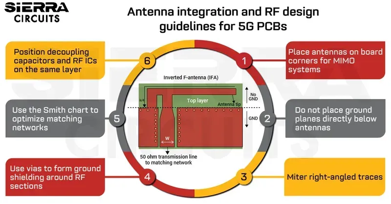
Integrating antennas directly onto the PCB is a critical design choice for wireless transmission modules, significantly impacting device form factor, cost, and overall RF performance. This intricate process demands meticulous attention to factors like antenna type, strategic placement to avoid interference, precise impedance matching for efficient power transfer, and optimization of the radiation pattern to ensure reliable signal coverage and regulatory compliance. Effective antenna integration on PCBs is pivotal for achieving optimal wireless communication, minimizing signal loss, and ensuring the module operates within its intended frequency spectrum with maximum efficiency.
What are the primary types of PCB integrated antennas? Common types of PCB integrated antennas include monopole, dipole, inverted F antenna (IFA), patch, and loop antennas. The selection depends on the operating frequency, required gain, physical space constraints, and desired radiation pattern for the specific wireless transmission module application.
How does antenna placement on the PCB affect performance? Antenna placement profoundly influences performance by affecting the radiation pattern, gain, and susceptibility to interference. Ideally, antennas should be placed at the edge or corner of the PCB, away from large ground planes or metallic components that can detune the antenna, shield the signal, or create unwanted reflections, leading to reduced efficiency and distorted radiation patterns.
Why is impedance matching crucial for PCB integrated antennas? Impedance matching ensures maximum power transfer from the RF circuitry to the antenna by minimizing signal reflections. A mismatch causes a portion of the signal to reflect back to the source, leading to power loss, reduced efficiency, increased heat generation, and potential damage to the RF front-end components. Typical target impedance is 50 ohms for most RF systems.
What is the significance of the antenna's radiation pattern? The radiation pattern describes how the antenna radiates or receives RF energy in different directions. Understanding and optimizing the radiation pattern is crucial for ensuring effective coverage and communication within the intended operational environment. A non-optimal pattern can lead to dead spots, reduced range, or interference with other devices.
Manufacturing and Assembly Processes for Wireless PCBs
Wireless PCB Manufacturing
The fabrication and assembly of Wireless Transmission Module PCBs demand a specialized approach, moving beyond standard PCB manufacturing to address the unique challenges of high-frequency signal integrity and precision. Ensuring high quality and reliability in these critical components hinges on stringent process control, advanced equipment, and expertise in handling delicate RF circuitry. This meticulous attention to detail from fabrication to final assembly is paramount to achieving optimal wireless performance and long-term device stability.
Why are specialized manufacturing processes crucial for Wireless Transmission Module PCBs? Specialized manufacturing processes are crucial because Wireless Transmission Module PCBs operate at high frequencies, making them highly susceptible to signal loss, interference, and impedance mismatches. Standard manufacturing methods often lack the precision required for tight tolerances, controlled impedance traces, and exact layer stack-ups, all of which are critical for maintaining signal integrity and RF performance. Specialized processes, like advanced material handling, precise etching, and vacuum lamination, mitigate these issues, ensuring consistent performance and reliability.
What unique challenges does the assembly of Wireless Transmission Module PCBs present? Assembly of Wireless Transmission Module PCBs faces unique challenges related to component sensitivity, thermal management, and solder joint integrity for RF components. Issues include precise placement of miniature RF components (e.g., filters, amplifiers, baluns), managing heat dissipation from power amplifiers without affecting signal performance, and ensuring robust solder connections that can withstand environmental stresses while maintaining low parasitic inductance and capacitance. Advanced soldering techniques, precise pick-and-place, and stringent quality checks are essential.
How does Zero One Solution Limited ensure quality in Wireless Transmission Module PCB manufacturing? Zero One Solution Limited ensures quality in Wireless Transmission Module PCB manufacturing through a multi-faceted approach. We employ advanced manufacturing equipment capable of ultra-fine line etching and precise layer alignment for impedance control. Our processes incorporate strict material handling protocols for high-frequency laminates, and we utilize automated optical inspection (AOI) and X-ray inspection for critical RF components and solder joints. Furthermore, our experienced engineers oversee every stage, from DFM analysis to final assembly, ensuring adherence to IPC standards and RF performance requirements.
What role does DFM play in the manufacturing of Wireless Transmission Module PCBs? Design for Manufacturability (DFM) plays a critical role in the manufacturing of Wireless Transmission Module PCBs by identifying and resolving potential manufacturing issues early in the design phase. For RF boards, DFM focuses on optimizing trace widths and spacing for impedance control, ensuring proper pad geometries for RF components, recommending suitable material stack-ups for high-frequency performance, and addressing potential thermal hotspots. This proactive approach minimizes costly re-spins, accelerates time-to-market, and significantly improves manufacturing yield and reliability.
What are the common pitfalls in assembling high-frequency wireless PCBs? Common pitfalls in assembling high-frequency wireless PCBs include improper handling of moisture-sensitive devices (MSDs), inconsistent solder paste application leading to voids or shorts, incorrect component placement causing impedance mismatches, and inadequate thermal profiles during reflow. These issues can lead to signal degradation, intermittent failures, and reduced overall performance. Addressing these requires a cleanroom environment, advanced pick-and-place accuracy, precise stencil design, and meticulous reflow oven calibration.
Testing and Validation of Wireless Transmission PCBs
Ensuring the reliability and optimal functionality of Wireless Transmission Module PCBs is paramount, and this is achieved through rigorous testing and validation protocols. These procedures are critical for verifying performance, ensuring compliance with industry standards, and identifying potential issues before mass production. A comprehensive testing strategy not only guarantees product quality but also mitigates costly failures and accelerates time-to-market, particularly for high-frequency RF designs where precision is key.
Why is testing critical for Wireless Transmission Module PCBs? Testing is critical for Wireless Transmission Module PCBs to ensure they meet specified performance parameters, comply with regulatory standards (e.g., FCC, CE), and function reliably in real-world scenarios. It helps identify design flaws, manufacturing defects, and signal integrity issues early, preventing costly recalls and enhancing product reputation. For high-frequency applications, even minor imperfections can lead to significant signal degradation, making meticulous validation indispensable for optimal wireless communication.
What are the key tests for Wireless Transmission Module PCBs? Key tests include Radio Frequency (RF) performance testing (e.g., transmit power, receiver sensitivity, spurious emissions), impedance matching verification using Time Domain Reflectometry (TDR), Signal Integrity (SI) analysis to check for reflections and crosstalk, power integrity (PI) analysis for stable voltage delivery, thermal testing to assess performance under varying temperatures, and environmental stress testing (e.g., humidity, vibration). Compliance testing, such as EMI/EMC, is also crucial for market readiness.
How does Zero One Solution Limited ensure the quality of Wireless Transmission Module PCBs? Zero One Solution Limited employs a multi-faceted approach to quality assurance for Wireless Transmission Module PCBs. This includes utilizing advanced Automated Optical Inspection (AOI) for defect detection, X-ray inspection for internal layer alignment and solder joint integrity, In-Circuit Testing (ICT) for component functionality, and Functional Circuit Testing (FCT) to simulate real-world operation. We also conduct specialized RF testing in controlled environments, leveraging our expertise in high-frequency design and manufacturing to ensure peak performance and reliability.
Zero One Solution Limited: Your Partner in PCB Solutions
Zero One Solution Limited stands as a premier PCB solution provider, particularly for the intricate demands of wireless transmission modules. Our deep expertise, honed over a decade, allows us to deliver end-to-end, high-quality, and rapid-response services, addressing the critical need for speed and precision in product development cycles. From initial design consultation through advanced manufacturing and assembly, we ensure that your wireless module PCBs are optimized for performance, reliability, and market readiness.
What sets Zero One Solution Limited apart in wireless PCB solutions? Our distinction lies in our specialized focus on rapid prototyping and our comprehensive, integrated approach. We offer a one-stop service covering PCB design, manufacturing, and assembly specifically tailored for wireless transmission modules. This streamlines your development process, significantly reduces time-to-market, and ensures seamless transitions between design iterations and production phases. Our strategic location in Shenzhen, coupled with a Dubai branch, leverages a global supply chain for unparalleled resource access and support.
How does Zero One Solution Limited ensure rapid prototyping for wireless modules? Our rapid prototyping capabilities are underpinned by advanced manufacturing facilities, efficient project management, and a dedicated team of experts. We utilize cutting-edge equipment for high-frequency material processing and employ agile methodologies to quickly iterate on designs. Our streamlined internal processes minimize delays, enabling us to deliver high-quality prototypes in record time, crucial for fast-paced R&D cycles in wireless communication.
Can Zero One Solution Limited handle complex RF layout challenges? Absolutely. Our veteran engineering team possesses extensive experience in complex RF layout techniques, crucial for optimal wireless performance. We meticulously address impedance control, signal integrity, electromagnetic interference (EMI) reduction, and antenna integration. We employ advanced simulation tools and adhere to rigorous design principles to ensure your wireless module PCBs perform optimally in challenging RF environments, minimizing signal loss and maximizing transmission efficiency.
In conclusion, the PCB is a cornerstone of successful wireless transmission modules, demanding careful attention to design, material selection, and manufacturing processes. Zero One Solution Limited offers comprehensive PCB solutions, from initial design to final assembly, ensuring that your wireless modules meet the highest standards of performance and reliability. We are committed to helping our clients accelerate their product development cycles and bring innovative wireless solutions to market with exceptional efficiency. Contact us today to discuss your project and discover how our expertise can empower your success in the world of wireless technology. Let Zero One Solution Limited be your trusted partner in PCB solutions, driving innovation and excellence in every connection.