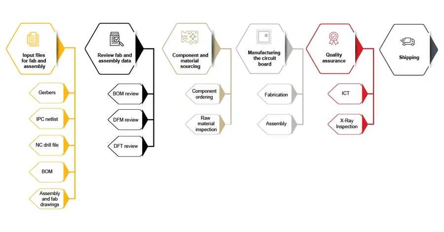
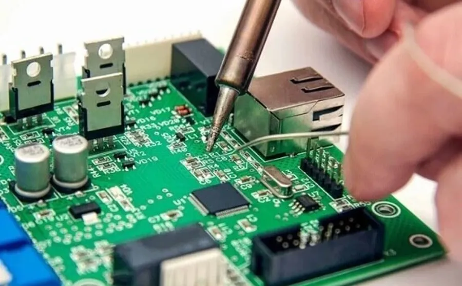
In today's fast-paced tech landscape, PCB (Printed Circuit Board) online services have become indispensable. They bridge the gap between innovative ideas and tangible electronics, simplifying PCB design, manufacturing, and assembly. This article will guide you through the myriad of online platforms, providing insights into how to leverage them for your projects, ensuring efficiency and quality in your PCB production journey.
Understanding PCB Online Platforms: An Overview
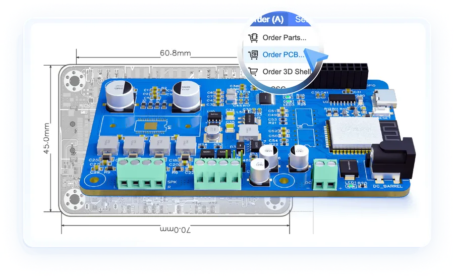
Online PCB Platform Interface
PCB online platforms provide a spectrum of services, encompassing manufacturing, design, and assembly, each catering to unique user needs with distinct advantages. These platforms have revolutionized the electronics industry, offering accessible, efficient, and often cost-effective solutions for bringing electronic designs to life.
Manufacturing Platforms These platforms focus on the fabrication of bare PCBs, transforming design files into physical boards. They offer various material options, layer counts, and finishes, catering to diverse project requirements. Key benefits include rapid prototyping, scalable production, and competitive pricing, often leveraging economies of scale. Examples include JLCPCB and PCBWay.
Design Platforms Online PCB design platforms provide tools and environments for creating circuit board layouts from schematics. These platforms offer features like component libraries, routing tools, and real-time design rule checks (DRC). Many are cloud-based, enabling collaborative design and version control. Key advantages are accessibility, ease of use, and collaborative capabilities. Examples include EasyEDA and Autodesk EAGLE (with cloud integration).
Assembly Platforms Assembly platforms provide services for populating bare PCBs with electronic components. These services can range from simple through-hole assembly to complex surface mount technology (SMT). They often include component sourcing, automated pick-and-place processes, and testing services. The key benefit is outsourcing of time-consuming and specialized assembly, reducing workload and improving production efficiency. Some manufacturers like JLCPCB and PCBWay offer integrated assembly services
Outsourcing of assembly, component sourcing, testing services
JLCPCB, PCBWay
Choosing the Right Online PCB Manufacturer
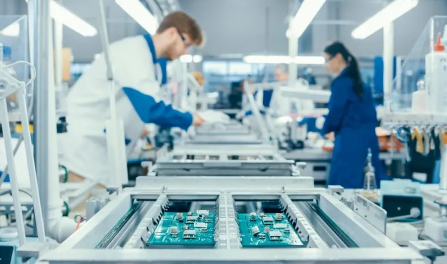
PCB Manufacturing Factory
Selecting the appropriate online PCB manufacturer is crucial for ensuring the success of any electronics project. This choice directly impacts the final product's quality, cost, and delivery timeline. A thorough evaluation of various factors is essential to identify a manufacturer that aligns with your specific project requirements.
Factor
Description
Importance
Pricing
Cost per PCB, considering quantity and complexity. Includes tooling, setup, and shipping.
Crucial for budget management; should be balanced with quality and other factors.
Turnaround Time
The duration from order placement to delivery of PCBs.
Vital for projects with tight deadlines; varies based on complexity and manufacturer workload.
Material Options
Selection of substrate materials (e.g., FR-4, Aluminum, Rogers), each with varying properties and cost.
Critical for application performance and reliability; material should be appropriate for operating environment.
Quality Certifications
Certifications like ISO 9001, UL, and IPC standards compliance indicate the manufacturer's quality control processes.
Essential to ensure the reliability and consistency of manufactured PCBs.
Minimum Order Quantity (MOQ)
The smallest batch of PCBs that a manufacturer will produce.
Important for cost and inventory planning, especially for small prototype runs.
Layer Count
Number of conductive layers on the PCB; important for circuit design complexity.
Must match design needs, more layers increase routing flexibility but adds cost.
Surface Finish Options
Variety of finishes such as HASL, ENIG, and OSP, chosen based on application and soldering method.
Affects soldering performance and shelf life of the boards.
Technology Capabilities
Manufacturer's ability to handle various technologies, such as blind/buried vias, impedance control, etc.
Required for complex designs and high-frequency applications; ensure capability matches project needs.
Shipping and Logistics
Shipping costs, delivery time and packaging options.
Impacts project timeline and total costs; consider international shipping implications if relevant
Customer Support
Ease of communication, responsiveness, and technical support offered by the manufacturer.
Important for a smooth production process, particularly for complex designs or first-time orders.
PCB Design Online: Tools and Workflow
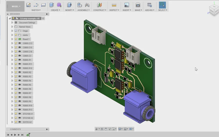
PCB Design Software Interface
Online PCB design platforms offer a range of software solutions, characterized by varying levels of user-friendliness, feature depth, and collaborative capabilities, facilitating efficient electronic design workflows.
These tools empower engineers to design circuit boards without the need for dedicated software installations, leveraging the cloud for accessibility and collaborative design.
User-Friendliness Online platforms often prioritize intuitive interfaces and simplified workflows to accommodate both novice and experienced designers. This includes drag-and-drop component placement, auto-routing features, and pre-designed library components.
Feature Sets Feature richness ranges from basic schematic capture and PCB layout to advanced simulations and design rule checks (DRC). Professional-grade features like differential pair routing, impedance control, and thermal analysis are frequently available, albeit sometimes at higher subscription tiers.
Collaboration Modern online PCB design tools promote teamwork through shared projects, real-time co-editing, and version control. These collaborative features enable effective communication and streamlined project management among team members.
Optimizing the online design workflow involves several critical steps:
Project Planning Clearly define the project requirements, including functionality, component selection, size constraints, and performance goals, before commencing the design process.
Schematic Capture Utilize the online tool to create a logical representation of the circuit. Ensure the schematic is accurate, well-organized, and consistent with your functional requirements. Double-check component footprints, pin assignments, and net connections.
PCB Layout Transform the schematic diagram into a physical PCB layout, carefully consider signal integrity, thermal management, component placement, and routing strategies. Adhere to best practices for minimizing noise, crosstalk, and electromagnetic interference (EMI). Use auto-routing tools cautiously, as manual adjustments are frequently needed for critical traces.
Design Rule Check Employ the tool's DRC feature to catch design errors like short circuits, inadequate spacing, and manufacturing rule violations. Address any warnings or errors before proceeding.
Gerber File Generation Create Gerber files, which represent the physical layers of your board. Confirm these files before submitting them for manufacturing, and verify the layer stackup and aperture settings.
Version Control Use the tool's built-in version control or an external system to track changes and allow smooth collaboration among team members.
By leveraging the available online resources, designers can streamline their workflow from initial concept to final PCB production. The key is to select tools that match specific requirements, prioritize user-friendliness, and incorporate collaborative features.
PCB Assembly Online: Streamlining Production
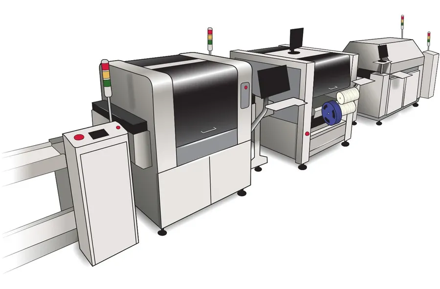
PCB Assembly Line
Online PCB assembly services are revolutionizing how electronic products are manufactured, offering a streamlined approach to component placement, soldering, and testing. These platforms provide access to sophisticated assembly capabilities, regardless of the project's scale, thereby democratizing the production of electronic devices.
Key aspects of online PCB assembly include:
Part Procurement Many online platforms offer component sourcing, simplifying the supply chain and ensuring the availability of parts for assembly. This often includes a wide selection of components from various manufacturers, with options for cost and availability optimization.
Surface Mount Technology (SMT) Assembly SMT is the predominant method for assembling modern PCBs, involving the precise placement and soldering of components onto the board. Online services typically utilize automated equipment, resulting in high-precision, high-volume capabilities, and the ability to handle complex designs with fine-pitch components.
Through-Hole Assembly While SMT is dominant, through-hole assembly is still necessary for certain components. Online platforms can accommodate through-hole components as well, either manually or with automated processes for larger pin counts, or special components.
Testing and Quality Control Reputable online assembly services provide testing options, including functional testing and visual inspection. These steps ensure the assembled PCBs meet design specifications and are ready for final integration.
To ensure efficient online assembly, designers should adhere to specific guidelines:
Design for Assembly (DFA) Optimize your board layout for efficient assembly by considering component orientation, spacing, and alignment. This reduces assembly errors, minimizes costs, and speeds up turnaround time. Adhering to these guidelines makes automated processes more accurate and cost-effective.
Gerber Files Submit clear and accurate Gerber files, including all necessary layers (copper, solder mask, silkscreen) and drill data. Ensure all files are correctly named and in the required format to prevent delays and errors in the manufacturing process.
Bill of Materials (BOM) Provide a comprehensive BOM with accurate part numbers, manufacturer names, and quantities. Using specific part numbers and manufacturer information allows the assembly service to source the exact components, avoiding compatibility or performance issues. Proper documentation is crucial for an efficient assembly process.
Component Footprints Ensure accurate component footprints in your design to avoid assembly issues. Double-check all component footprints match the manufacturer specifications before submitting for assembly. Incorrect footprints lead to misalignment, poor solder joints, and potential functional failures.
Panelization When ordering multiple boards, consider panelization for efficient assembly. Panelization arranges multiple copies of the PCB on one manufacturing panel, streamlining the production process and lowering costs. Verify the panelization process is in accordance to the manufacturer’s guidelines.
Choosing the right online PCB assembly service involves understanding the specific needs of your project, along with the capabilities of various platforms. Consider factors such as assembly complexity, production volume, and required testing, when making your selection.
Cost Comparison of PCB Online Services
Navigating the costs of PCB online services requires a clear understanding of the various factors that influence pricing. This section provides a comprehensive analysis of cost structures across different PCB online platforms, offering a comparative look at manufacturing, assembly, and design services. By understanding these cost drivers, users can make informed decisions tailored to their specific project requirements and budget constraints.
Service
Cost Factors
Typical Cost Range
Notes
PCB Manufacturing
Board size, layer count, material type, quantity, turnaround time
$5 - $500+ per board
Costs can vary significantly based on complexity and volume.
PCB Assembly
Number of components, SMT vs. through-hole, complexity of assembly, part procurement, testing
$0.05 - $1.00+ per component
Cost per component decreases with higher volumes.
PCB Design
Complexity of design, design software, hourly rate or flat fee
$50 - $200+ per hour / $100 - $5000+ per project
Freelance designers may have different fee structures than design firms.
The following are critical factors influencing PCB online service costs:
- Board Size & Complexity: Larger boards and higher layer counts typically increase costs due to material consumption and manufacturing complexity.
- Material Type: Standard FR-4 is typically the most cost-effective material, whereas specialty materials like Rogers or flex circuits can significantly increase costs.
- Component Quantity: The number of components and the assembly method (SMT or through-hole) directly affect the final assembly cost.
- Turnaround Time: Expedited or rush services usually come at a premium, while standard or longer lead times offer cost savings.
- Quality Certifications: PCB manufacturers that provide ISO or other certifications may charge slightly more, but this can be an important consideration for higher reliability needs.
- Part Procurement: If a manufacturer procures your components, expect additional costs compared to providing your own parts for assembly.
When selecting a provider, it is crucial to consider not only the direct costs but also the associated trade-offs in terms of turnaround time, design complexity, and quality requirements. Comparing costs across multiple providers is always recommended to optimize budget and project objectives. Note that free online PCB design tools do not come without costs; these costs typically are in the form of limited functionality and advertising, but can be an economical solution for simpler projects.
Frequently Asked Questions About PCB Online Services
This section addresses common inquiries regarding PCB online services, providing clear and concise answers to help users navigate the world of online PCB manufacturing, design, and assembly.
What does PCB stand for? PCB stands for Printed Circuit Board. It is a fundamental component in most electronic devices, providing mechanical support and electrical connections for electronic components through conductive pathways.
Can I learn PCB design on my own? Yes, you can absolutely learn PCB design independently. Numerous online resources, tutorials, and software platforms offer comprehensive learning paths. Start with basic electronics and CAD software and then practice with real-world projects. Discipline and dedication are key for self-learners.
Why can some PCBs be manufactured so cheaply? The cost of PCB manufacturing has significantly decreased due to advancements in automation, economies of scale, and efficient global supply chains. Online platforms facilitate streamlined production processes. However, extremely low-cost options often involve trade-offs in material quality, manufacturing tolerances, or delivery times. It is crucial to understand the cost drivers when choosing a manufacturer.
How much does PCB manufacturing typically cost? PCB manufacturing costs vary widely depending on factors such as board dimensions, layer count, material type, minimum trace width/spacing, quantity, and chosen manufacturer. Simple single-layer boards can be very inexpensive, while complex multi-layer PCBs with high precision requirements will command higher prices. It is best to request a quote based on your project's specific needs.
What are the common file formats required for ordering PCBs online? The most common file format for ordering PCBs is Gerber files (.gbr, .gbx, .cmp, .sol, etc), which are industry-standard for PCB manufacturing. You will also need a drill file (.drl) for hole locations, and sometimes a netlist file (.net) for design validation. Many platforms also support direct uploads of PCB design software files like Eagle, KiCad, or Altium.
How do I choose the right PCB material for my project? The material selection for your PCB depends heavily on the application. FR-4 is the most common, offering a good balance of cost and performance. For higher performance applications, you might choose materials like polyimide or Rogers for better temperature stability, dielectric constant, and signal integrity characteristics. Consider the operating environment and performance needs before selecting the material.
Online PCB Order Process: A Step-by-Step Guide
Online PCB Order Process
Ordering PCBs online involves a systematic approach to ensure accuracy and efficiency. This section provides a detailed, step-by-step guide to navigate the process, covering PCB manufacturing, design, and assembly. The focus is on preparing your files correctly, selecting appropriate options, and completing your order successfully.
Step 1: Prepare Your Design Files Ensure your PCB design files are in the correct format (e.g., Gerber files for manufacturing, design files for modification). Use PCB design software to export the necessary files. Double-check for any errors or inconsistencies before proceeding. This is often the most critical step as incorrect files will lead to manufacturing errors.
Step 2: Choose Your Online PCB Service Select a PCB online platform that matches your needs. Consider factors such as cost, turnaround time, material options, and available technologies. Look for platforms with clear pricing and customer support options to ensure you receive guidance when necessary.
Step 3: Upload Your Files and Select Options Upload your prepared files to the chosen platform. Then specify your PCB requirements, including dimensions, material (e.g., FR4, aluminum), layer count, copper thickness, solder mask color, silk screen and surface finish. The ability to customize this step is usually crucial to achieving the desired PCB performance.
Step 4: Review and Approve Your Order Carefully review the summary of your order. This includes a detailed breakdown of costs, chosen specifications, and delivery timeframe. Correct any errors immediately before confirming. This step also includes often a final preview of the layout to confirm accuracy.
Step 5: Complete Your Purchase and Await Delivery Proceed to the payment stage and complete the online purchase. Make note of your order ID. After this, the PCB manufacturer will produce your boards. They will provide you with a tracking number once they have shipped. Delivery times will vary depending on shipping options.
Tips for Optimizing Your PCB Online Experience
Assembled PCBs
To maximize efficiency and success when utilizing online PCB services, careful attention to detail in file preparation, effective communication with manufacturers, and diligent review of feedback are crucial. These elements directly impact the quality, cost, and turnaround time of your PCB projects.
File Preparation Best Practices Ensure all design files are in the correct format (e.g., Gerber, ODB++), and that they are complete and accurate. Double-check layer alignments, drill files, and silkscreen information. Use the manufacturer's design rule check (DRC) tool prior to submission to catch any potential issues early.
Communication with Manufacturers Maintain clear and concise communication with the manufacturer. Clearly specify your requirements, including material specifications, tolerances, special finishes, and desired performance. If any clarification is needed, do not hesitate to ask questions before finalizing your order. Consider time zone differences if communicating with overseas manufacturers.
Understanding and Utilizing Feedback Pay close attention to any feedback provided by the manufacturer. Address any concerns or issues promptly and work with them to resolve any discrepancies. Learn from each experience and refine your designs accordingly.
Standardize your design process Use consistent layer naming conventions, keep track of all the changes you make to your design. This process will help you avoid errors and improve the efficiency of future projects.
Plan Your Project Timeline Effectively Consider the manufacturing time and shipping estimates. Factor in buffer time for potential delays due to issues with the designs, manufacturer production issues, or shipping challenges. Starting your order well in advance of when the finished PCBs will be needed allows you to work around unforeseen problems effectively.
Double-Check Your Order Details Before confirming your online PCB order, always double-check every detail. This includes the materials used, quantity, PCB thickness, copper weight, finish, and any other technical requirements.
Future Trends in PCB Online Services
The PCB online service landscape is poised for significant evolution, driven by advancements in technology and shifting industry demands. These trends will impact not only how PCBs are designed and manufactured but also the overall user experience within online platforms.
AI-Driven PCB Design Tools The integration of Artificial Intelligence (AI) and Machine Learning (ML) into PCB design software will revolutionize the process. AI algorithms will automate routing, placement, and optimization tasks, reducing design time and complexity. These tools will also aid in predictive analysis, identifying potential design flaws before manufacturing.
Enhanced Material Options The future will see a wider selection of advanced materials available through online platforms, including those with improved thermal conductivity, flexibility, and high-frequency performance. This will cater to increasingly specialized applications, such as aerospace, automotive, and wearable technology.
Streamlined Manufacturing Processes Online PCB manufacturing is expected to further streamline, leveraging automation and real-time monitoring. This involves optimized production flows, predictive maintenance of equipment, and enhanced quality control via machine vision systems. This will lead to faster turnaround times and lower costs.
Digital Twins for PCB Manufacturing The concept of digital twins will become more prevalent. Creating digital replicas of physical PCBs enables simulation, testing, and validation before actual production, reducing potential errors and enhancing manufacturing predictability and efficiency.
Increased Focus on Sustainability The PCB industry is expected to move towards more sustainable practices. Online services will likely promote eco-friendly materials, offer recycling options, and minimize waste through optimized production. This aligns with the global emphasis on environmentally conscious manufacturing.
Integration of Cloud-Based Platforms Cloud computing and the internet of things (IoT) technology will play an increasingly large role. All aspects of PCB design, manufacturing, and assembly will be performed within interconnected systems. Collaboration between designers, manufacturers, and assemblers will be greatly improved using cloud-based platforms that can be accessed globally.
The world of PCB online offers a plethora of opportunities for designers and engineers to bring their ideas to life with enhanced efficiency and reduced overhead. By leveraging the right online platforms, you can streamline your PCB design, manufacturing, and assembly process. As technology advances, look for more innovative ways [pcb online] services will integrate into your product development cycle, making it faster and cheaper to go from concept to reality.