Your Guide to Low-Cost PCB Fabrication: From Prototype to Production
2025.01.08
In today's rapid-paced tech landscape, low cost PCB fabrication is essential for innovation, whether you're an engineer, hobbyist, or a large-scale manufacturer. This article breaks down the complexities of PCB fabrication, providing a clear roadmap for achieving high-quality results without breaking the bank. We'll explore various cost-effective strategies, from selecting the right materials to choosing the ideal fabrication partners, ultimately empowering you to bring your electronics projects to life affordably.
Understanding the Factors Influencing PCB Fabrication Costs
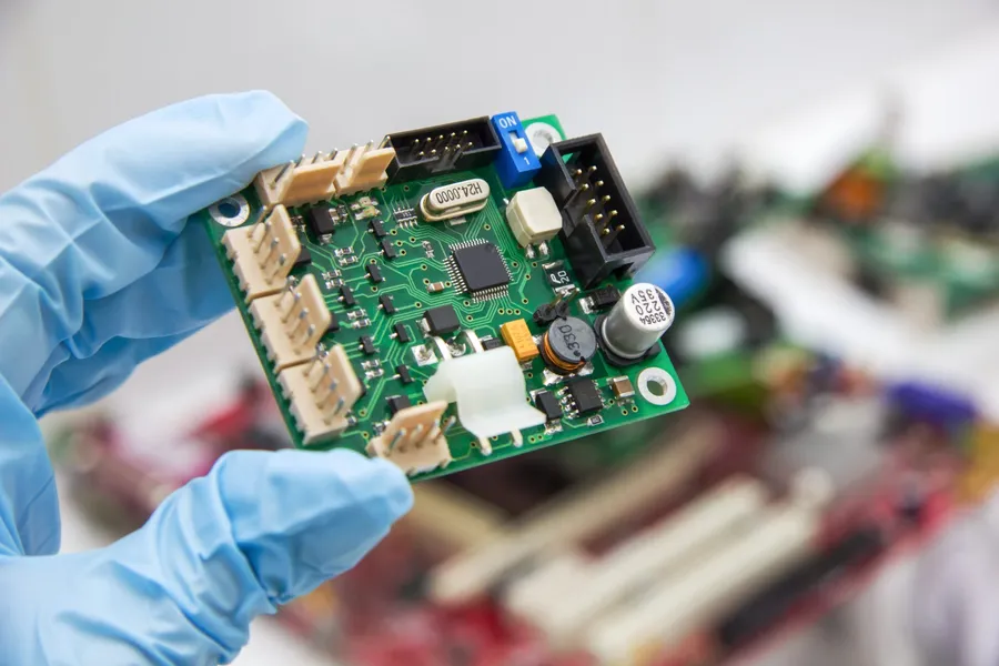
Printed Circuit Board
PCB fabrication costs are determined by a multitude of interconnected factors, each contributing significantly to the final price. These factors span from the physical characteristics of the board to the complexities of its design and the manufacturing requirements. A comprehensive understanding of these elements is critical for engineers and designers aiming to optimize their budgets.
Board Size and Dimensions Larger boards inherently require more material and processing time, increasing the overall cost. The area of the PCB directly correlates with material usage and the necessary processing steps.
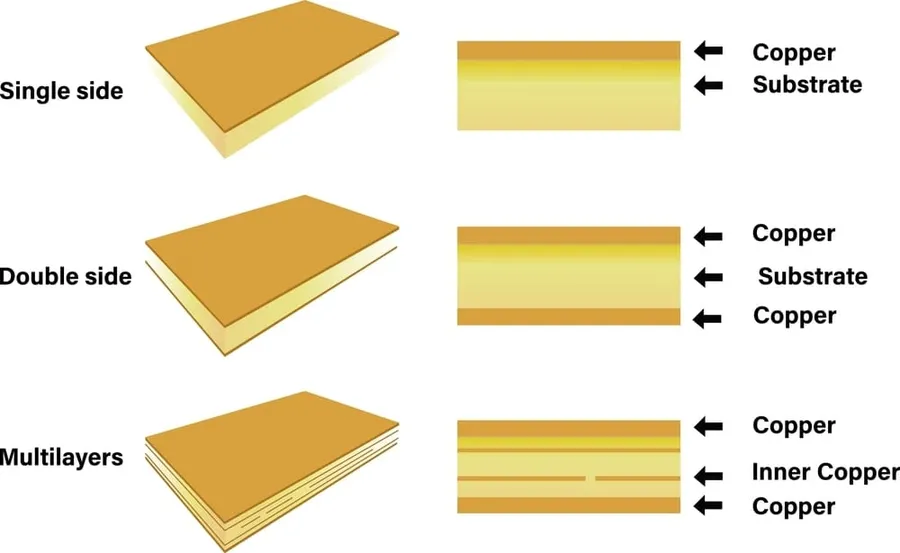
Number of Layers Multi-layer PCBs, with their complex internal routing and connections, demand sophisticated production processes, resulting in elevated costs compared to single or double-sided boards. Each added layer involves additional material costs and lamination procedures.
Material Type The choice of substrate, such as the widely used FR-4, influences costs. Advanced materials like aluminum-backed PCBs or high-frequency laminates will escalate expenses due to specialized processing and material costs. The selection of a specific material must be carefully assessed for its cost and performance requirements.
Order Quantity Bulk orders benefit from economies of scale, resulting in lower per-unit prices. Smaller quantities may incur higher costs, as tooling setup and administrative expenses can be distributed across a smaller number of units. For prototype orders it is typically more expensive.
Lead Time Expedited production schedules or rush orders attract premium pricing. Standard lead times are more cost-effective and should be selected when time is not a primary concern. The urgency and speed of delivery will influence pricing.
Design Complexity Intricate designs with a high number of vias, small trace widths, and tight clearances increase manufacturing challenges, driving up costs. The more complex the design is, the more precise and labor-intensive the manufacturing will be.
Surface Finish The surface finish (e.g., HASL, ENIG, OSP) not only impacts the solderability of the PCB but also affects cost. More advanced finishes like ENIG are typically more expensive than standard HASL or OSP. The choice of surface finish should consider both performance and cost.
Specialized Features Specialized fabrication requirements or added processes can contribute to increased manufacturing costs. Special features might include blind and buried vias, controlled impedance traces, and specific routing and milling requirements.
Low-Cost PCB Fabrication Techniques for Prototypes
PCB Prototypes
Prototyping PCBs on a budget requires strategic choices in design and manufacturing. Prioritizing simplicity and utilizing cost-effective techniques can significantly reduce expenses without sacrificing functionality during the initial stages of development. Focus on design choices that lower manufacturing complexities. This approach reduces the cost of each board, enabling more iterations and flexibility in the prototyping phase.
Single-Sided Boards Opting for single-sided PCBs is the most straightforward and economical approach for prototypes. This design eliminates the need for plated through-holes and complex layer alignment, thereby lowering fabrication costs and complexity.
Standard Layer Counts For prototypes requiring more complexity, sticking to two-layer boards is a cost-effective choice. While multilayer PCBs offer greater functionality, the increase in manufacturing complexity adds considerable cost. Two-layer boards offer a good balance between cost and functionality for many applications.
FR-4 Material FR-4 is a standard and widely used substrate material due to its affordability and good electrical insulation properties. It is a suitable choice for most prototype applications as its ubiquitous availability keeps costs down. Consider other substrates only when the application absolutely requires it.
Larger Via Sizes Using larger via sizes (e.g., 0.3mm or greater) makes the manufacturing process less demanding and reduces costs. Smaller vias require more precise drilling and plating, which will increase fabrication costs.
Simplified Design Rules Adopting simplified design rules, including wider trace widths and clearances, can lower the cost of manufacturing. Complex designs with fine traces and tight clearances require tighter tolerance control, increasing the expense of fabrication. For prototypes, prioritize cost and rapid iteration over ultra high density designs.
Panelization While not always applicable for very low quantity prototyping, panelization, especially when coupled with standard sizes provided by the manufacturer, can often lower per board cost by increasing the efficiency of the manufacturing process. It groups several PCBs together to utilize the full area of the manufacturing panels
Choosing the Right PCB Manufacturer: A Comparison
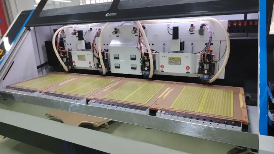
PCB Factory
Selecting the appropriate PCB manufacturer is a critical step in ensuring both the quality and cost-effectiveness of your project. This section provides an objective comparison of popular low-cost PCB fabrication services, namely PCBWay, JLCPCB, and OSH Park. We will delve into their pricing structures, lead times, available services, and quality control measures to equip you with the knowledge to make an informed decision based on your specific needs.
Feature
PCBWay
JLCPCB
OSH Park
Pricing Structure
Variable, based on complexity and quantity. Offers discounts for larger quantities.
Generally lower prices for standard PCBs. Cost-effective for prototypes and small runs.
Fixed price per square inch, which simplifies cost estimation. Suitable for smaller boards.
Lead Times
Typically 2-7 days for manufacturing. Shipping time varies based on location and method.
Fast manufacturing, often 2-3 days. Shipping times are similar to PCBWay.
Slower manufacturing lead times, typically 12-15 business days. Shipping time depends on your region.
Available Services
Offers a wide range of services, including SMT assembly, CNC machining, and stencil production.
Focuses on PCB fabrication and assembly with options for SMT assembly and stencils.
Primarily PCB fabrication, doesn't provide in-house assembly services.
Quality Control
Has a reputation for strong quality control, employs rigorous checks during fabrication.
Offers good quality at lower price points, includes electrical testing.
Known for high-quality boards and consistent fabrication, but has a higher cost per board area.
Minimum Order Quantity
Variable. Smallest quantities are possible, but are the most expensive.
Generally 5 PCBs for prototypes. Higher quantities will reduce the unit cost.
Three copies of each PCB design is the standard minimum. Price is per board, not per square inch.
Material Options
Wide variety of materials, including FR-4, aluminum, and flexible PCB materials.
Primarily FR-4 but with options for different thicknesses and copper weights.
Primarily FR-4 standard thickness, with copper weighting options available.
Frequently Asked Questions About Low-Cost PCB Fabrication
Navigating the world of low-cost PCB fabrication can be complex, with many factors influencing the final price. This section addresses the most common questions to provide clear and concise answers, helping you make informed decisions for your PCB projects.
What is the cheapest way to make a PCB? The most cost-effective method for PCB fabrication typically involves using single-sided boards, standard FR-4 material, and larger via sizes with minimal design complexity. Opting for simpler designs and standard layer counts significantly reduces manufacturing costs. Additionally, batching orders for multiple PCBs together can lower per-unit prices. DIY methods such as etching can be cheapest for single prototypes but lack the precision of professional fabrication and have high setup time per unit.
How much does it cost to get a PCB assembled? PCB assembly costs vary significantly based on factors such as the number of components, the complexity of the board, the type of components (SMT vs. through-hole), and the assembly method (manual vs. automated). Smaller, simpler boards with a limited number of components are less expensive to assemble. Assembly costs can range from a few cents per component to several dollars per board for complex designs. Considering DFM (Design for Manufacturing) during the design phase helps reduce assembly costs.
What is the most cost-effective PCB finish? The most budget-friendly PCB surface finish is typically HASL (Hot Air Solder Leveling), a lead-based or lead-free solder finish. HASL offers good solderability and is widely available. However, if RoHS compliance is mandatory, lead-free HASL is required, which may be slightly more expensive than leaded. Other finishes such as ENIG (Electroless Nickel Immersion Gold) offer better performance and shelf life but come at a higher price. Choosing HASL when appropriate will minimize fabrication costs.
How to calculate PCB fabrication cost? Calculating PCB fabrication costs involves considering numerous factors: board size, the number of layers, material type, quantity, lead time, and specific design features such as vias, surface finish, and special requirements. PCB manufacturers provide online quote calculators or quote tools that allow you to input your specific design parameters and obtain an estimate. Always factor in set-up costs, which can make small batches more expensive per unit. It's essential to accurately specify all your requirements to get an accurate quote.
Are there any free PCB design software options available? Yes, several free PCB design software options are available. KiCad is a powerful open-source software that is popular amongst hobbyists and professionals. EasyEDA offers a browser-based environment, and Autodesk Eagle has a free personal-use license. These tools provide comprehensive features for creating PCB layouts and schematics without incurring software costs. Choosing free software can help reduce overall project expenses.
What are the benefits of panelizing PCBs for low-cost fabrication? Panelizing PCBs for fabrication, combining multiple boards into a single panel, offers several cost-saving benefits for larger orders. This approach reduces manufacturing time and costs by allowing efficient use of material and production processes. Furthermore, panelization provides for simpler pick and place assembly, further reducing costs. When ordering larger quantities, panelization helps to achieve lower per-unit costs.
How can I reduce the cost of PCB prototypes? To reduce the cost of PCB prototypes, focus on simplifying designs, using standard component sizes and footprints, using standard FR-4 material, larger via sizes, choosing HASL surface finish and keeping the board size as small as possible. Ordering in small quantities can often be more expensive per-unit, and therefore try to order enough prototypes to get the bulk price breaks. It is also important to review and compare quotes from multiple manufacturers to secure the best prices.
Cost-Effective Material Selection for PCBs
PCB Materials
The selection of materials significantly impacts the final cost of printed circuit boards (PCBs). This section provides a focused analysis of how substrate, copper thickness, and surface finish choices influence PCB production expenses, offering practical guidelines for balancing cost and performance.
Understanding the material implications is crucial for both prototype and production PCB design. Selecting the most cost-effective options, while maintaining the required functionality, is a key part of optimizing your project budget.
Material Property
Impact on Cost
Considerations for Cost Optimization
Substrate Material
High cost associated with advanced materials; FR-4 is the standard, but alternatives like CEM materials offer cost savings.
Use FR-4 for most standard applications; consider CEM-1 or CEM-3 for non-critical applications with cost constraints.
Copper Thickness
Thicker copper increases material cost and requires more processing time and materials.
Select standard 1 oz (35µm) copper thickness for most applications; avoid unnecessarily thick copper which increases costs significantly.
Surface Finish
ENIG (Electroless Nickel Immersion Gold) is a more expensive finish. HASL (Hot Air Solder Leveling) is a lower cost finish.
Use HASL for most applications. Consider ENIG for better solderability and longer shelf-life, but the increase in price should be justified.
Material selection should be considered at the earliest design phase to avoid additional costs. For prototypes, the use of cost-effective materials, without excessive features, is critical. For production runs, these considerations will result in substantial savings. By applying these principles, both cost and design objectives can be achieved.
Design for Low-Cost Manufacturing: Best Practices
PCB Layout
Efficient PCB design is paramount for minimizing fabrication costs. By adhering to specific design principles, one can significantly reduce manufacturing expenses without compromising functionality. These practices focus on simplifying the production process, thereby lowering both material usage and manufacturing time.
Utilize Standard Component Footprints Opt for widely available and standard component footprints. These are often readily available in PCB design software libraries, reducing the need for custom footprints which can increase design time and cost. Using standard footprints simplifies component placement and reduces errors during assembly.
Optimize Trace Widths and Clearances Employ minimum trace widths and clearances according to your chosen manufacturer's capabilities. Adhering to the manufacturer's recommended design rules for trace widths and spacing can minimize fabrication issues. A slightly wider trace and larger clearance will avoid any issues at the manufacturer, and will not increase the cost. Overly fine traces and tight spacing will often increase costs.
Avoid Unnecessarily Complex Features Minimize the use of complex features such as microvias and blind vias when possible. While these may be necessary in some situations, they increase the fabrication cost. Standard through-hole vias are the cheapest to manufacture and should be used if possible. Simplify the design of the layers and their connections where possible, as this makes fabrication simpler and cheaper.
Minimize the Number of Layers Keep the number of layers as low as possible. Double-sided boards are more cost effective than multi-layered PCBs, as each added layer increases cost. Only add layers if necessary to add functionality.
Use Larger Via Sizes Standard and slightly larger via sizes are less expensive to fabricate than microvias. Larger sizes will be more reliable and reduce the chance of the drill bit wandering, or breaking, during fabrication.
Panelize Designs for Efficiency When ordering multiple boards, consider panelizing them. Panelization reduces manufacturing costs, as they are fabricated and assembled as one panel, which improves the cost per board. Your manufacturer can provide details about the size and requirements of their panels.
For example, a simple microcontroller board can be designed using a two layer board, standard through-hole vias, and with minimum trace widths and clearances. This is the cheapest way to fabricate a board. Using a surface-mount version of the same microcontroller will still cost roughly the same, however, a board with very small traces, multiple layers, and microvias, is more expensive. Therefore, the design choices made during the design phase, greatly impact the final manufacturing costs.
Optimizing for Volume Production: Scaling Low-Cost PCB Manufacturing
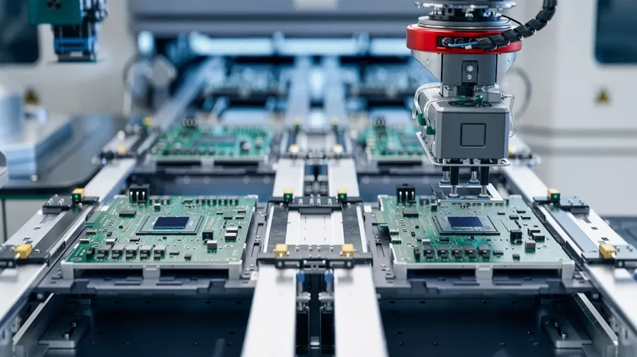
PCB Mass Production
Transitioning from prototyping to volume production requires a shift in focus from individual board costs to per-unit costs, which can be significantly reduced by leveraging economies of scale. This section explores strategies such as volume discounts, panelization, and selecting manufacturers with the right scaling capabilities to achieve cost-effective large-scale PCB manufacturing.
Volume Discounts Most PCB manufacturers offer tiered pricing based on order quantity. As the quantity increases, the per-unit cost decreases. Negotiate pricing based on estimated annual volume to secure the best rates.
Panelization Panelization involves combining multiple individual PCBs onto a single manufacturing panel. This significantly reduces handling costs, minimizes material waste, and accelerates production throughput. Consider common panel sizes that align with your manufacturer's capabilities to optimize material usage.
Manufacturer Selection for Scaling Choose manufacturers with experience in handling large-volume orders, possess automated assembly lines, and have robust quality control mechanisms. Check reviews and feedback of their past customers. Manufacturers who offer a full suite of services, from fabrication to assembly, can streamline the process and lead to considerable savings.
Cost saving examples: Let's consider a PCB design that requires 1000 units. If the per unit cost for a small order (5-10 units) of that same board is \$5, ordering it at a larger scale can reduce the unit cost by 50-70% based on the manufacturing company, hence bringing the cost down to \$1.5 - \$2.5/unit. This reduction can be achieved by negotiating with the manufacturer and applying optimized panelization. Another way to reduce cost is by using a manufacturer with assembly capabilities, reducing the logistic of separate manufacturing and assembly by combining it as a single job.
Optimization Strategy
Description
Cost Reduction Impact
Volume Discounts
Lower per-unit price as order quantity increases
Significant (10-70%) reduction in per-unit cost
Panelization
Combining multiple PCBs onto a single manufacturing panel
Moderate (5-15%) reduction in manufacturing costs
Optimized Manufacturer Selection
Choosing manufacturers with capacity for large volume production
Moderate (5-20%) reduction in total costs
Comparing PCB Fabrication Options
Choosing the right PCB fabrication service is crucial for balancing cost and quality. This section provides a detailed comparison of popular low-cost PCB manufacturers, focusing on key parameters, materials, and features, empowering informed decision-making based on specific project needs. The table below highlights the strengths and weaknesses of each manufacturer.
Feature
JLCPCB
PCBWay
OSH Park
Base Material
FR-4, Aluminum, Rogers
FR-4, Aluminum, Rogers, Flexible
FR-4
Layer Count
1-16 Layers
1-32 Layers
Up to 4 Layers
Minimum Track/Space
4mil/4mil
3mil/3mil
6mil/6mil
Surface Finish
HASL, ENIG, OSP
HASL, ENIG, Immersion Silver, OSP
ENIG
Turnaround Time
24 Hours - 7 Days
24 Hours - 10 Days
1-2 Weeks
Cost (5 Boards)
Very Low
Low - Medium
Medium
Shipping
Variable, Express Options Available
Variable, Express Options Available
Standard, US only
Quality Control
Automated Optical Inspection
Automated Optical Inspection, Electrical Testing Available
Visual Inspection
Additional Services
SMT Assembly, Stencil Service
SMT Assembly, CNC Machining, 3D Printing
None
Strategies for Minimizing PCB Assembly Costs
Reducing PCB assembly costs is crucial for both prototyping and mass production. This section outlines effective strategies, focusing on component selection, assembly partner choices, design guidelines, and the utilization of open-source tools to minimize expenses at each stage of the PCB assembly process.
Component Selection Opt for standard, readily available components to reduce costs. Unique or hard-to-source parts often come with price premiums and longer lead times. Consider using components with common footprints to allow for flexibility in sourcing and assembly.
Assembly Partner Selection Carefully evaluate potential assembly partners based on their pricing structures, experience with similar projects, and the level of automation in their processes. Choose an assembly partner whose service capabilities align with your project's requirements and cost constraints.
Design for Assembly (DFA) Guidelines Implement DFA principles in your PCB design. This involves optimizing component placement for efficient pick-and-place processes, using consistent component orientations, and minimizing the number of unique components. Effective DFA can significantly reduce assembly time and errors, ultimately lowering costs.
Open Source SMT Stencils Utilize open-source SMT stencil designs to save on tooling costs. Many online resources provide freely available designs, or customizable templates that can drastically lower the cost of the stencil for solder paste application.
Assembly Partner
Pricing Structure
Lead Time
Specialization
Key Advantages
Company A
Tiered pricing based on quantity and complexity
2-7 business days
High-mix, low-volume production
Flexibility, good for prototype runs
Company B
Competitive flat rate per PCB
7-14 business days
High-volume, automated assembly
Cost-effective for large production runs
Company C
Customized quotes based on project
3-10 business days
Specialized in complex component placement
Ideal for sophisticated boards requiring advanced SMT techniques
Achieving low cost PCB fabrication is entirely feasible by understanding the underlying factors influencing expenses and adopting strategic planning in design and material selection. Whether you're prototyping a new invention or scaling up production, this guide provides the necessary information to help navigate the complexities of PCB fabrication. Armed with this knowledge, you can bring innovative electronics projects to fruition while staying within budget and fostering creativity and growth in the realm of electronics. Remember, low cost doesn't mean low quality - informed choices lead to great results.