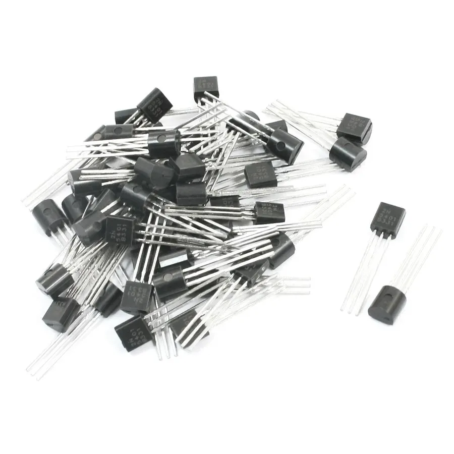
2N5401 Transistor: A Comprehensive Guide to its Applications and Uses
2025.02.03
The 2N5401 transistor, a humble component in the world of electronics, plays a crucial role in numerous applications from simple amplifiers to complex switching circuits. It's a PNP type transistor, known for its ability to handle high voltages. Just as a traffic signal directs the flow of cars, the 2N5401 directs the flow of current, making it a fundamental part of many circuits. This article delves deep into understanding the 2N5401, its workings, and how it compares to other similar transistors, providing you with the knowledge to effectively implement it in your electronic projects.
Understanding the 2N5401 PNP Transistor
2N5401 Transistor
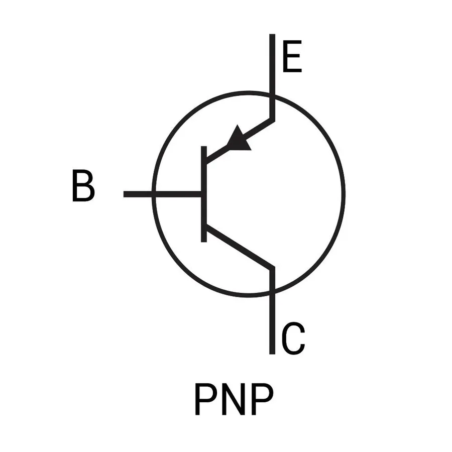
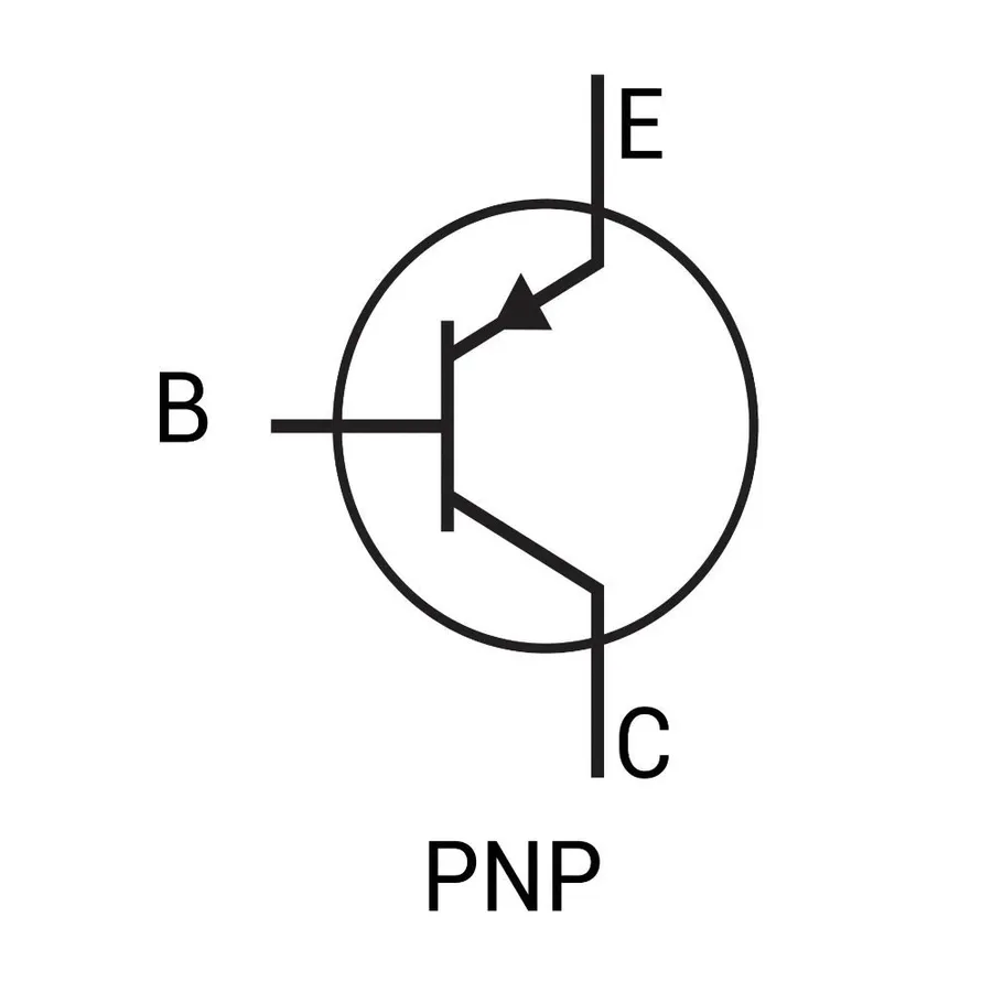
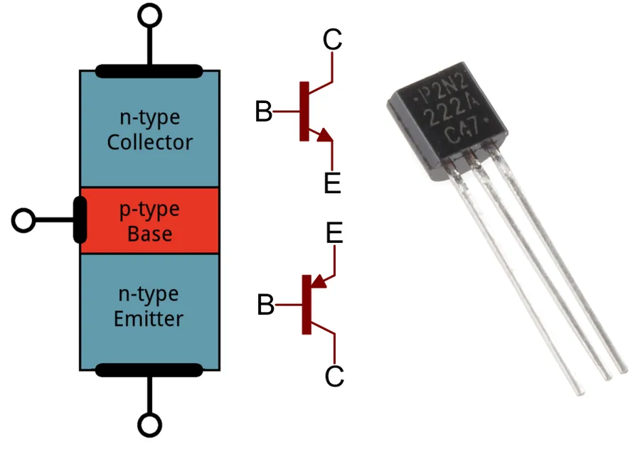
The 2N5401 is a widely utilized PNP bipolar junction transistor (BJT), distinguished by its construction and suitability for high-voltage applications. Its operation relies on the manipulation of current flow between its three terminals—the base, collector, and emitter—through the application of a small current at the base, enabling it to function as an electronic switch or amplifier. This capability makes it an integral component in numerous electronic circuits, particularly where high voltage handling and amplification are required.
Key Specifications and Parameters of the 2N5401
The 2N5401 transistor, a PNP bipolar junction transistor, is characterized by several key parameters that dictate its performance in electronic circuits. Understanding these specifications is crucial for effective circuit design and ensuring reliable operation. These parameters are typically found within the 2N5401 datasheet.
Parameter
Symbol
Value
Unit
Description
Collector-Emitter Voltage
VCEO
160
V
Maximum voltage that can be applied between the collector and emitter without damaging the transistor.
Collector-Base Voltage
VCBO
180
V
Maximum voltage allowed between the collector and base terminals.
Emitter-Base Voltage
VEBO
6
V
Maximum voltage that can be applied between the emitter and base without damaging the transistor.
Collector Current (Continuous)
IC
600
mA
Maximum continuous current the collector can handle.
Peak Collector Current
ICM
1
A
The maximum current allowed for short durations.
Power Dissipation
PD
625
mW
Maximum power the transistor can dissipate without damage, often dependent on ambient temperature and package type.
Operating Junction Temperature
TJ
150
°C
Maximum temperature the transistor junction can reach during operation.
Storage Temperature Range
TSTG
-65 to +150
°C
Temperature range within which the transistor can be stored without damage.
DC Current Gain (hFE)
hFE
40 to 240
Ratio of collector current to base current, indicates the transistor's amplification ability.
Transition Frequency
fT
50
MHz
Frequency at which the current gain drops to unity, a measure of high-frequency performance.
2N5401 Pinout and Configuration
2N5401 Pinout
The 2N5401 transistor, housed in the TO-92 package, is a three-terminal device with a specific pin configuration critical for circuit design. Understanding this pinout—identifying the Base, Collector, and Emitter—is fundamental for its proper use in electronic circuits. The correct connections of these pins are essential to ensuring the transistor functions as intended.
The TO-92 package is a common through-hole package for small signal transistors. When viewed from the front (the flat side of the transistor facing you), and with the leads facing downwards, the pins are arranged as follows, from left to right:
Emitter The leftmost pin is the Emitter. This terminal emits or injects charge carriers into the base region.
Base The center pin is the Base. This terminal controls the current flow between the collector and emitter.
Collector The rightmost pin is the Collector. This terminal collects the charge carriers.
The following diagram illustrates this pin configuration for the 2N5401 in the TO-92 package:
It's crucial to note that the orientation of the transistor is essential, and incorrect wiring can lead to malfunction or even damage to the component or circuit. Always double-check the datasheet or relevant material for proper pin identification.
Typical Applications of the 2N5401 Transistor
Transistor Circuit
The 2N5401 transistor, a versatile PNP bipolar junction transistor, finds utility across diverse electronic applications, primarily due to its high voltage handling capabilities and moderate current gain. Its characteristics make it suitable for high-voltage switching, small signal amplification, and as a driver for more complex circuit components.
High-Voltage Switching The 2N5401 excels in high-voltage switching circuits, where it acts as an electronic switch to control the flow of current in response to a control signal. This capability is crucial in power electronics and control systems. For instance, it can be used to switch higher voltage loads such as relays or solenoids.
Small Signal Amplification With its moderate gain characteristics, the 2N5401 is well-suited for amplifying weak signals, such as those from sensors or audio transducers. In pre-amplifier circuits, the transistor boosts the signal level, making it more suitable for processing and driving subsequent stages of a signal chain.
Driver Circuits The 2N5401 serves as an effective driver for other circuit elements that require higher power or current. As a driver, the transistor acts as a bridge, providing the necessary current to control or activate a relay, motor, or other higher-power components. This role is essential in many control and actuation circuits. For example, it can drive a relay that operates an indicator light.
2N5401 vs. 2N5551 and other Equivalent Transistors
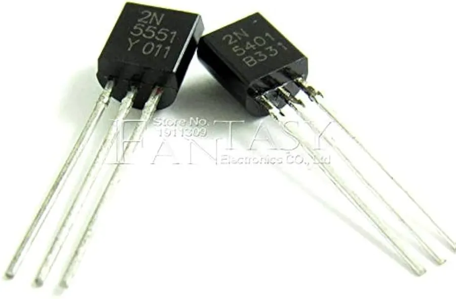
2N5401 vs 2N5551
The 2N5401 is a widely used PNP bipolar junction transistor, but understanding its alternatives is crucial for design flexibility and cost optimization. This section provides a comparative analysis between the 2N5401 and other common transistors like the 2N5551, A1015, and 2N4401, highlighting their key differences in specifications and suitable applications.
Parameter
2N5401 (PNP)
2N5551 (NPN)
A1015 (PNP)
2N4401 (NPN)
Polarity
PNP
NPN
PNP
NPN
Collector-Emitter Voltage (VCEO)
-150V
160V
-50V
40V
Collector Current (IC)
-600mA
600mA
-150mA
600mA
Power Dissipation (PD)
625mW
625mW
400mW
625mW
Transition Frequency (fT)
50 MHz
300 MHz
80 MHz
100 MHz
Typical Application
High-voltage switching, small signal amplification
High-frequency amplification, switching
General-purpose amplification
General-purpose switching
The 2N5401 is a PNP transistor, while the 2N5551 and 2N4401 are NPN transistors. The A1015 is also a PNP transistor. The 2N5401 offers a high VCEO of -150V, making it suitable for high-voltage applications. The 2N5551 has a similar IC and PD but differs in its polarity and has a higher fT, which makes it suitable for high frequency applications. The A1015, while also a PNP, has significantly lower current and power capabilities. The 2N4401 is an NPN transistor with a lower VCEO but similar current and power ratings. The selection of an equivalent transistor depends heavily on the specific circuit requirements, with polarity being the most critical factor. When selecting an alternative, care should be taken to consider the specific design needs, with particular focus on the polarity, voltage, current, and frequency specifications of the circuit. This approach ensures that the chosen alternative will provide the desired functionality in the specific application. If a PNP is required, the A1015 or a similar PNP is often used. If an NPN is required, the 2N5551 or 2N4401 might be suitable.
Practical Considerations When Using the 2N5401
The 2N5401, while a robust PNP transistor, requires careful consideration of several practical factors to ensure reliable and safe operation in electronic circuits. These considerations span from thermal management to proper circuit design practices and component selection.
Heat Management The 2N5401, like all transistors, generates heat during operation, particularly when switching high currents or at higher voltages. It is crucial to manage this heat to prevent damage or premature failure. This may involve using a heat sink, employing forced air cooling, or designing the circuit to minimize power dissipation. The maximum junction temperature is a critical parameter, and exceeding it can lead to device failure. Datasheets provide thermal resistance specifications, which are critical for determining heat sink requirements. For instance, the thermal resistance from the junction to ambient for a TO-92 package is typically quite high, necessitating careful thermal considerations.
Circuit Design Proper circuit design is paramount for ensuring the 2N5401 operates within its safe operating area (SOA). This involves selecting appropriate resistor values, capacitor values, and operating points to avoid overstressing the transistor. For example, ensuring that the base current does not exceed the maximum rating is crucial. Furthermore, when using the 2N5401 in switching applications, it's essential to consider rise and fall times to minimize power dissipation during switching transients. Impedance matching between stages can optimize performance and reduce noise.
Selecting Supporting Components The performance and reliability of a circuit using the 2N5401 are significantly influenced by the quality and specifications of the surrounding components. For example, when using the 2N5401 as a switch, selecting a base resistor that provides adequate current to drive the transistor into saturation is essential while not exceeding its maximum base current. The use of appropriate bypass capacitors can improve circuit stability. The voltage and current ratings of all components must be adequate for the specific application. Using lower-rated components can lead to component failure or system malfunctions.
Precautions During Handling The 2N5401 is a sensitive semiconductor device and can be damaged by electrostatic discharge (ESD). Therefore, it is important to use proper grounding techniques when handling the transistor to avoid accidental damage. Storing the transistors in ESD-safe bags or containers is recommended. Avoid using excessive force on the pins during insertion into a circuit and do not subject the device to excessive heat (soldering). Overheating during soldering can cause internal damage, affecting the transistor's performance and reliability.
Dealing with Heat Dissipation When the 2N5401 operates at higher currents or voltages, heat dissipation becomes a critical consideration. Without proper heat management, the transistor's junction temperature can rapidly exceed its maximum rating, leading to potential thermal runaway and device failure. The use of heat sinks is common to dissipate the heat. The choice of heat sink depends on the amount of heat generated and the operating environment. For more demanding applications, forced-air cooling, or liquid cooling may be necessary.
Frequently Asked Questions About the 2N5401 Transistor
This section addresses common inquiries about the 2N5401 transistor, providing concise and informative answers to help you understand its applications, alternatives, and operational characteristics. We aim to resolve typical user doubts, offering practical guidance for utilizing this component effectively.
What is the primary use of a 2N5401 transistor? The 2N5401 is primarily used as a high-voltage PNP transistor in switching and amplification circuits. Its characteristics make it suitable for applications requiring medium power handling and moderate current gain, such as small signal amplifiers and high-voltage switching.
What are some common equivalent transistors for the 2N5401? The 2N5551, A1015, and 2N4403 are common equivalents for the 2N5401. When selecting an equivalent, you should compare key parameters like VCEO, IC, hFE and power dissipation to ensure the replacement component meets the circuit requirements. The 2N4401 is an NPN transistor and is NOT an equivalent of the PNP 2N5401.
Can a 2N4401 transistor be used as an equivalent for the 2N5401? No, a 2N4401 transistor cannot directly replace a 2N5401. The 2N4401 is an NPN transistor, while the 2N5401 is a PNP transistor. They have opposite polarities and different circuit configurations. A direct substitution would require a circuit redesign, including the appropriate biasing and current directions.
Is it safe to replace any transistor with another transistor? No, it is not advisable to replace a transistor with just any other transistor. Transistors have specific ratings and characteristics (such as voltage, current gain, polarity, and power). Replacing one with a non-equivalent type might lead to component failure, circuit malfunction, or even damage to other circuit parts. Careful consideration must be given to parameter matching and polarities.
What should I consider when selecting a 2N5401 replacement? When choosing a 2N5401 replacement, the most important factors to consider are: similar polarity (PNP), Collector-Emitter Voltage (VCEO), Collector Current (IC), current gain (hFE) and Power Dissipation (PD) ratings. Always consult the datasheets for the original and replacement components to ensure that the parameters are within the acceptable range for the application. Also, check the package type and pin configuration to ensure mechanical compatibility.
What are the key differences between a 2N5401 and a 2N5551 transistor? Both the 2N5401 and the 2N5551 are popular bipolar junction transistors, but the 2N5401 is a PNP type, while the 2N5551 is an NPN type. The 2N5551 has a higher maximum collector current and a lower collector-emitter saturation voltage than the 2N5401. These differences influence how each component will operate in a circuit. Always use the datasheet to guide your component selection.
Are there any precautions I should take when using a 2N5401? Yes, you should take several precautions: Ensure proper heat management, particularly when the transistor is operating at or near its maximum rated power. Use appropriate biasing to ensure that the transistor is operating within its safe operating area (SOA). Do not exceed any maximum ratings (VCEO, IC, PD, etc.) specified in the datasheet. Always handle transistors with care to avoid electrostatic discharge (ESD), which may damage the component.
Where to Buy 2N5401 Transistors and Cost Considerations
2N5401 Transistor Packaging
The 2N5401 transistor, while not the most cutting-edge component, remains readily available through a variety of distributors due to its continued use in legacy and niche applications. Understanding where to source these transistors, and at what price, is crucial for both hobbyists and professional engineers.
Key factors influencing the cost of 2N5401 transistors are the quantity purchased, the supplier's reputation, and whether the components are genuine or sourced through less reliable channels. Bulk purchases generally result in lower per-unit costs, making it more economical for larger production runs. Reputable distributors typically charge a premium for assured quality and traceability of components.
Major Electronic Component Distributors Companies like Digi-Key, Mouser Electronics, and Arrow Electronics are reputable sources for purchasing 2N5401 transistors. They offer a wide selection of components, detailed datasheets, and reliable supply chains. These distributors often cater to both small and large orders.
Online Marketplaces Platforms such as Amazon, eBay, and AliExpress also list 2N5401 transistors. However, care should be taken to verify the seller’s legitimacy and component authenticity. Prices may be competitive, but quality can be inconsistent.
Local Electronic Stores Brick-and-mortar electronic component stores may stock 2N5401 transistors, offering immediate availability. This can be a viable option for small quantities or for urgent projects. However, pricing may be less competitive than online distributors.
Direct Manufacturers For very large volume orders, it may be economical to approach semiconductor manufacturers directly. This ensures component authenticity and potentially lower pricing, although it requires significant purchase volumes and direct negotiation.
Factor
Description
Impact on Price
Quantity Purchased
The total number of transistors ordered
Price per unit typically decreases with larger quantities.
Distributor Reputation
The standing and trustworthiness of the supplier
Reputable distributors may charge a premium for guaranteed quality.
Component Authenticity
Whether the transistors are genuine or counterfeit
Authentic components may cost more but offer reliability and performance.
Shipping Cost and Speed
The method and time required for delivery
Shipping costs can significantly impact the total price, especially for small orders.
How to Test a 2N5401 Transistor
Testing a 2N5401 transistor with a multimeter is a crucial step in verifying its functionality before incorporating it into a circuit. This process ensures the transistor isn't damaged or faulty, preventing potential circuit malfunctions. The following outlines the steps to perform this test.
Preparation Ensure the multimeter is set to diode test mode or resistance mode (typically ohms, Ω). It's best to remove the transistor from the circuit or ensure the circuit is powered off to avoid erroneous readings or damage to the meter.
Identifying the Transistor Leads Correctly identify the transistor leads as base (B), collector (C), and emitter (E). Refer to the 2N5401 datasheet or pinout diagrams to confirm the layout, which is typically, from left to right, Emitter, Base, Collector when facing the flat side of a TO-92 package. This is critical for accurate testing.
Testing the Base-Emitter Junction Place the positive (red) lead of the multimeter on the base (B) and the negative (black) lead on the emitter (E). You should observe a voltage drop of approximately 0.6 to 0.7 volts (V) in diode test mode or a low resistance value in resistance mode, indicating the base-emitter diode is forward biased. Reversing the leads should show no current flow (OL or very high resistance).
Testing the Base-Collector Junction Keep the positive (red) lead on the base (B) and move the negative (black) lead to the collector (C). Similar to the base-emitter junction, you should observe a voltage drop of approximately 0.6 to 0.7V or a low resistance value, indicating a forward bias across the base-collector junction. Reversing the leads should show no current flow (OL or very high resistance).
Testing the Collector-Emitter Junction Place the positive (red) lead on the collector (C) and the negative (black) lead on the emitter (E). This junction should exhibit a very high resistance in both directions, meaning no current should pass. A low resistance reading suggests the transistor is likely shorted and faulty. Ensure the leads are clean to ensure a proper connection.
Interpretation of Results If the junctions behave as described above, it indicates the transistor is likely functional. If any of the junctions show low resistance in both directions, or an unexpected open circuit, it indicates the transistor is faulty and should be replaced. When using a multimeter to verify, the readings must be interpreted carefully.
The 2N5401 transistor, with its high-voltage capability and versatile applications, remains a workhorse in the field of electronics. Understanding its properties, limitations, and use-cases is crucial for any electronics enthusiast or engineer. From its role as a simple switch to part of complex circuits, the 2N5401 provides a vital function, and knowledge of this transistor will empower you to build more effective and reliable electronics projects. This understanding also opens the door to the deeper world of transistor technology and the possibilities it holds.