
In the fast-evolving world of automotive connectivity, telematics gateways serve as the nerve center for vehicle data. As signal speeds climb and board real estate shrinks, traditional design methods are no longer sufficient. This guide navigates the essential DFM protocols required to maintain signal integrity in dense, multi-layer gateway systems, ensuring your designs meet the rigorous reliability standards of the automotive industry.
Understanding the High-Speed Gateway Challenge
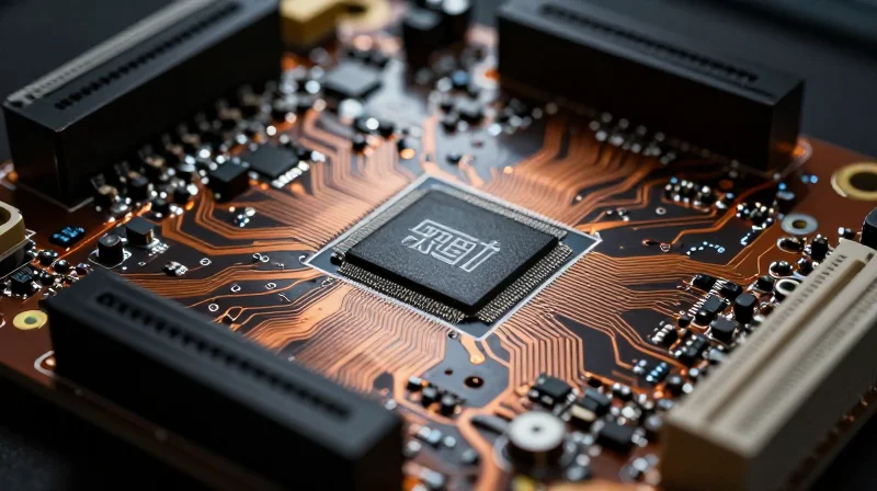
The Convergence of Telematics and High-Density Design
The evolution of the automotive telematics gateway has transformed from a simple cellular bridge into a complex high-performance computing node. As these systems move toward autonomous integration, they must process multi-gigabit data streams from V2X (Vehicle-to-Everything) communications, 5G NR (New Radio), and integrated infotainment systems simultaneously. This convergence forces designers to adopt high-density interconnect (HDI) technologies, creating a critical challenge: achieving signal integrity at high frequencies without compromising the manufacturability or thermal reliability of the PCB.
Core Engineering Challenges
- Signal Integrity vs. Density
As data rates climb, minimizing cross-talk and insertion loss requires precise trace geometries and impedance control, which often conflict with the need for high-component-density routing. - Thermal Management Demands
High-performance processing chips generate significant heat that must be dissipated through the board, necessitating advanced thermal via stitching and strategic copper pours that complicate standard DFM assembly protocols. - Regulatory Compliance
Automotive-grade PCBs must adhere to stringent ISO 26262 functional safety standards, meaning every DFM choice—from layer stackup to solder mask definition—must be validated for long-term vibration and thermal cycling resistance.
| Requirement | Design Impact | DFM Constraint |
|---|---|---|
| 5G Connectivity | High-frequency losses | Low-loss substrate selection |
| Component Density | Routing complexity | Micro-via and via-in-pad usage |
| Harsh Environment | Mechanical fatigue | Optimized copper balancing |
Ultimately, the challenge lies in the 'manufacturing window.' Designing for high-speed performance is meaningless if the board cannot achieve high yields during fabrication. Bridging the gap between electrical design simulation and manufacturing capability requires early-stage engagement with fabrication partners to validate stackup constraints, via aspect ratios, and material thermal coefficients before the design is locked.
Strategic Stack-up Design for Signal Isolation
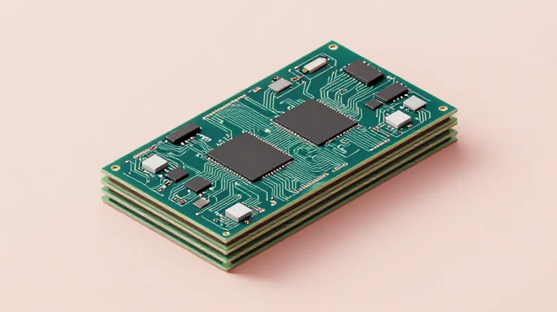
Strategic Stack-up Configuration
Optimizing stack-up design for automotive telematics is a balancing act between signal integrity (SI) and thermal management. A robust stack-up must prioritize ground plane proximity for high-speed signals to minimize return path inductance and provide adequate shielding for sensitive RF traces.
| Design Factor | Recommendation | Justification |
|---|---|---|
| Layer Pairing | Ground-Signal-Ground | Ensures continuous return path and EMI containment |
| Core Thickness | Thin Dielectrics (<= 3 mil) | Maximizes coupling between planes for planar capacitance |
| Isolation | Separate RF and Digital | Prevents crosstalk between noisy processing units and sensitive receivers |
EMI Mitigation and Reference Plane Integrity
To achieve high-speed signal integrity in an automotive environment, reference planes must remain contiguous. Any break in a ground plane underneath a high-speed differential pair creates an impedance discontinuity and emits electromagnetic radiation. For automotive gateways, it is standard practice to implement stitching vias along the perimeter of high-speed transmission lines to create a 'Faraday cage' effect.
Stack-up Design Best Practices FAQ
- Why is planar capacitance important in automotive stack-ups?
Planar capacitance acts as a high-frequency decoupling reservoir, reducing power distribution network (PDN) impedance and suppressing voltage noise in high-speed processors. - How does core thickness affect impedance control?
Thinner cores allow for narrower trace widths while maintaining target impedance, which is essential for high-density routing in compact telematics modules. - When should I use buried vias for signal isolation?
Buried vias are recommended when switching layers for high-speed signals to minimize stubs that can cause resonance and signal degradation in multi-gigahertz applications.
Managing Controlled Impedance in Multi-layer Boards
Geometric and Material Dependencies
Controlled impedance is a function of trace width, copper thickness, dielectric height, and the dielectric constant (Dk) of the substrate. For automotive telematics, where high-speed signals like Gigabit Ethernet and LVDS are prevalent, even minor variations in these parameters can lead to significant signal reflections and timing jitter.
| Parameter | Influence on Impedance | Design Consideration |
|---|---|---|
| Trace Width | Inverse | Maintain ±10% tolerance during etching |
| Dielectric Height | Direct | Strict control over prepreg thickness |
| Dielectric Constant (Dk) | Inverse | Use stable, low-loss materials like Megtron 6 |
| Copper Thickness | Inverse | Account for plating buildup in final width |
Manufacturing Tolerances and Best Practices
Standard manufacturing tolerances are often insufficient for high-speed automotive gateways. Designers must collaborate with fabrication houses to ensure impedance targets of 50-ohm single-ended and 100-ohm differential signals are met despite process variations.
- How does copper etch factor affect impedance?
During the etching process, the sides of the trace are eroded, creating a trapezoidal cross-section; failing to compensate for this 'etch factor' will result in higher-than-target impedance. - Why is material selection critical for automotive?
Automotive environments involve extreme thermal cycling; using materials with a stable Dk across temperature ranges prevents impedance drift and maintains signal integrity over the vehicle's lifespan. - What role does the reference plane play?
A continuous, unbroken reference plane is essential; any crossing of split planes creates a path of high impedance, leading to massive signal radiation and EMI failures.
Design Verification Workflow
1. Run 2D field solver simulations early in layout.
2. Define impedance coupons on board rails for destructive testing.
3. Verify Dk values provided by the PCB manufacturer.
4. Apply etching compensation factors to Gerber design files.
Mitigating Crosstalk through Geometric Optimization

Advanced Geometric Mitigation Strategies
To maintain signal integrity in automotive telematics, designers must move beyond basic design rules and adopt aggressive geometric optimization. Crosstalk, primarily driven by the mutual capacitance and inductance between adjacent nets, can be drastically reduced through precise control of trace geometry and spatial relationships.
- 3W Rule Application
Enforce a minimum spacing of three times the trace width between critical signal lines to ensure the electric field lines primarily terminate on the reference plane rather than neighboring conductors. - Via Stitching and Guarding
Place grounded via stitching along high-speed signal paths to create a localized Faraday shield, effectively containing EMI and limiting the coupling coefficient between parallel runs. - Parallel Length Constraints
Limit the coupling length of parallel trace runs by periodically alternating routing layers or introducing zig-zag geometries to prevent the accumulation of phase-aligned crosstalk energy.
Comparison of Crosstalk Reduction Techniques
| Technique | Mechanism | Manufacturing Complexity |
|---|---|---|
| Increased Spacing | Reduces mutual capacitance | Low |
| Reference Plane Proximity | Forces tight field return | Medium |
| Guard Traces | Intercepts fringe fields | High |
| Differential Routing | Common-mode rejection | Medium |
Frequently Asked Questions on Trace Geometry
- Does increasing the dielectric height help with crosstalk?
No, increasing dielectric height actually increases the loop area for return currents, which usually worsens crosstalk. Lower dielectric heights are preferred to keep the field tightly bound to the reference plane. - When should guard traces be used?
Guard traces are recommended when spatial constraints prevent the use of the 3W rule, particularly in highly congested areas of the telematics gateway board.
Advanced Via-in-Pad and Transition Design
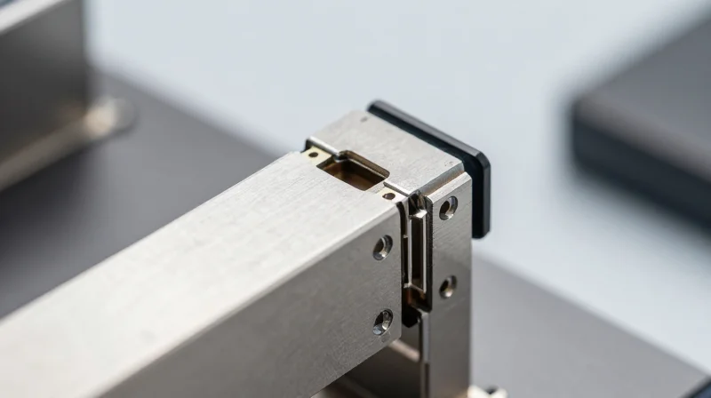
Strategic Implementation of Via-in-Pad Plated Over (VIPPO)
In high-speed automotive telematics, traditional dog-bone routing introduces excessive stub length and parasitic inductance, which are fatal to multi-gigabit data streams. Implementing Via-in-Pad Plated Over (VIPPO) allows for direct connection from the BGA pad to the inner layers, significantly reducing signal transition geometry. To ensure DFM compliance, manufacturers require specific processes: the via must be drilled, electroless copper plated, plugged with conductive or non-conductive epoxy, and then over-plated with copper to create a flat, solderable surface.
Transition Optimization Guidelines
| Design Parameter | Standard Practice | High-Speed Recommendation |
|---|---|---|
| Via Pad Diameter | 12-16 mil | 8-10 mil (Laser drilled) |
| Anti-pad Clearance | Standard | Increased to minimize capacitive loading |
| Back-drilling | Optional | Required for signals > 5 Gbps |
Addressing Common Via-in-Pad Challenges
- How do we prevent solder wicking into the via?
The use of an effective planarization process during the copper capping stage is essential to ensure the pad is fully sealed, preventing solder from entering the barrel and creating a bridge or weak joint. - What is the impact of back-drilling on transition performance?
Back-drilling removes the unused portion of the via barrel (the stub), which acts as an open-ended transmission line causing resonant reflections. Eliminating these stubs is mandatory for maintaining signal integrity in high-frequency automotive gateways. - Why is anti-pad optimization critical for VIPPO?
The anti-pad (clearance in the reference plane) creates a discontinuity in the return path. Adjusting the anti-pad size helps compensate for the excessive capacitance introduced by the via pad, maintaining a consistent 100-ohm differential impedance through the transition.
Addressing Return Path Discontinuities
Minimizing Return Path Impedance Mismatches
A high-speed signal’s return path seeks the path of least impedance, which is directly beneath the signal trace. When a reference plane is split—often by thermal reliefs, connector cutouts, or anti-pads—the return current is forced to diverge, creating massive loop inductance and radiated EMI. To address this, designers must ensure an uninterrupted solid copper ground plane reference for all high-speed signals, specifically those operating in the multi-gigabit range.
Stitching Strategies for Discontinuities
When signals must cross a reference plane split or transition between layers, the current path must be preserved using stitching vias. These 'stitching' connections provide a low-impedance bridge for the return current to follow the signal transition, effectively reducing the loop area. Proper placement of these vias must be as close to the signal via as possible, typically within a radius of 20-30 mils.
| Scenario | Risk Factor | Mitigation Strategy |
|---|---|---|
| Plane Split Crossing | High Inductive Loop | Add Bridge Capacitor or Stitching Vias |
| Layer Transition | Reference Change | Place Ground Stitching Vias at Via Exit |
| Connector Cutout | Signal Reflection | Minimize Void Size; Maintain Plane Underpins |
Frequently Asked Questions
- Why is a bridge capacitor used over plane splits?
A high-frequency decoupling capacitor (typically 10nF to 100nF) acts as an AC short, allowing return currents to bypass the split while maintaining DC isolation between power domains. - How many stitching vias are required for a signal transition?
While one is the absolute minimum, a pair or a quad-pattern surrounding the signal via is recommended to ensure the return path impedance remains stable and symmetrical. - Do I need to worry about return paths on low-speed signals?
Return path discontinuities are primarily critical for high-speed edge rates where the current must follow the trace closely to avoid excessive radiation; low-speed signals are less sensitive but good layout practice should still apply.
DFM Verification: Simulation to Fabrication
The Simulation-to-Fabrication Feedback Loop
The transition from virtual design verification to physical production is the most critical phase in the DFM workflow for automotive telematics. Discrepancies between idealized simulation environments and real-world manufacturing tolerances often lead to signal integrity degradation. Designers must utilize post-layout verification tools that extract real parasitic data from ODB++ or IPC-2581 files, accounting for variables like resin distribution, copper thickness variations, and etching factors.
| Simulation Parameter | Manufacturing Variable | Risk if Ignored |
|---|---|---|
| Dielectric Constant (Dk) | Glass Weave Effect | Signal Skew/Jitter |
| Copper Roughness | Surface Treatment | Insertion Loss Spike |
| Trace Impedance | Etch Factor/Profile | Signal Reflections |
Best Practices for Early Fabrication Engagement
Early collaboration with fabrication partners is not merely a courtesy; it is a technical necessity. By performing a design-for-fabrication (DFF) review during the pre-layout stage, engineers can align their stack-up requirements with the fabricator's process capabilities. This prevents issues such as uncontrolled impedance due to improper laminate selection or manufacturing-induced signal attenuation.
- Stack-up Alignment
Confirm the availability of specific high-speed laminates and verify the fabricator's ability to achieve precise dielectric thicknesses required for tightly controlled differential pairs. - Panelization Efficiency
Define panelization early to optimize grain direction, ensuring that high-speed traces are aligned consistently to mitigate variations in glass weave influence on signal propagation. - Drill/Via Tolerance
Establish drill-to-copper clearances that accommodate the fabricator’s registration tolerances, reducing the risk of broken return paths or insufficient clearance at layer transitions.
Verification FAQ
- Why should I use post-layout simulation?
It accounts for actual geometry, via parasitics, and routing nuances that pre-layout models estimate, providing an accurate prediction of hardware performance. - How does glass weave affect high-speed signals?
Non-uniform fiberglass distribution causes localized impedance changes, potentially leading to differential pair skew and eye-diagram degradation at 10Gbps+ speeds.
Meeting Automotive Reliability Standards (AEC-Q100)
Designing for AEC-Q100 Compliance
AEC-Q100 certification is not merely a testing phase but a design mandate. For high-speed telematics gateways operating in harsh automotive environments, reliability is governed by the ability of the PCB to withstand extreme temperature cycling, vibration, and humidity. Designers must prioritize materials with high Glass Transition Temperatures (Tg) and low Coefficient of Thermal Expansion (CTE) to prevent pad cratering and via fracture during the product's extended lifecycle.
| Reliability Factor | Design Strategy | Impact on Performance |
|---|---|---|
| Thermal Cycling | High Tg (>170°C) Laminates | Prevents delamination under thermal stress. |
| CTE Mismatch | Controlled Z-axis Expansion | Reduces stress on barrel-to-pad interfaces. |
| Vibration/Shock | Rigid-Flex/Reinforced Stackups | Improves mechanical robustness of interconnects. |
Key Considerations for Interconnect Integrity
- Why is copper elongation important?
AEC-Q100 standards demand high-ductility copper to ensure via barrels do not crack during repetitive thermal expansion cycles common in engine bay environments. - How does surface finish affect reliability?
ENIG is often avoided due to the 'black pad' risk; high-reliability designs prefer ENIPIG or Immersion Silver with robust oxidation protection to maintain bond strength. - What role does signal integrity simulation play?
Simulation must account for environmental drift in dielectric constants (Dk/Df), ensuring that high-speed signals remain within jitter and eye-mask specifications across the entire operating temperature range.
Ultimately, AEC-Q100 success rests on the synergy between material science and layout precision. By implementing balanced stackups that minimize mechanical stress and validating high-speed traces against temperature-dependent dielectric variations, designers ensure that telematics gateways meet the stringent quality gates required for modern vehicle connectivity.
Achieving signal integrity in high-speed automotive gateways is a balancing act of precision engineering and manufacturing foresight. By strictly adhering to these DFM rules, you can significantly reduce prototyping cycles and ensure your hardware delivers peak performance in the field. Ready to optimize your next design? Contact our engineering team today to review your project specifications and ensure your gateway hardware is built for success.
