
As modern electronics demand smaller footprints and higher performance, the complexity of printed circuit board design has shifted into the realm of 10 to 32 layers. Designing for such density without compromising yield requires more than just standard software rules—it demands a deep understanding of manufacturing tolerances, thermal management, and signal integrity. In this guide, we break down the critical DFM protocols to ensure your complex designs translate perfectly from CAD to the cleanroom.
The Anatomy of High-Layer Stackup Design
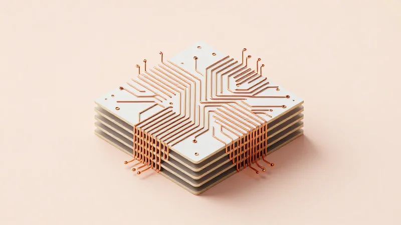
Principles of Symmetric Stackup Architecture
For high-density interconnect (HDI) boards exceeding 10 layers, symmetry is the primary defense against mechanical failure. A balanced stackup ensures that the thermal expansion forces are equalized above and below the neutral axis of the board. Deviating from a mirrored construction—where core and prepreg materials are identical in thickness and orientation relative to the center—inevitably leads to board twist and bow during the reflow process.
Material Selection Criteria: Tg and CTE
Material selection for high-layer counts focuses on managing the Coefficient of Thermal Expansion (CTE) and the Glass Transition Temperature (Tg). High Tg materials (typically >170°C) are essential to prevent structural degradation during repeated soldering cycles. When aligning materials, designers must match the CTE of the dielectric to the copper foils to minimize interlaminar stress.
| Parameter | Requirement for 20+ Layers | Impact of Failure |
|---|---|---|
| Tg | 170°C - 180°C | Pad lifting and delamination |
| CTE (Z-axis) | < 3.0% (50-260°C) | Via barrel cracking |
| Copper Distribution | ±5% variance | Mechanical warpage |
Copper Balancing and Warpage Prevention
Uneven copper density creates localized stress points that manifest as permanent board deformation. Designers should employ a 'copper pouring' strategy to fill empty areas, ensuring that the copper-to-dielectric ratio remains consistent across both the X and Y axes of every layer pair.
- How does layer count impact warpage?
As layer count increases to 32, the cumulative effect of thickness variation becomes exponential; symmetric foil weights and dielectric distribution are mandatory. - What is the role of the neutral axis?
The neutral axis represents the board's center. All design features, including copper weight and substrate thickness, must be mirrored around this axis to neutralize bending moments.
Mastering Controlled Impedance in Dense Layers

Mastering Controlled Impedance in Dense Layers
In multilayer boards ranging from 10 to 32 layers, maintaining impedance stability is no longer just about trace geometry; it involves mitigating the interaction between high-speed signals and the PCB laminate structure. As board density increases, the margin for error in dielectric constant (Dk) stability and manufacturing tolerances diminishes, necessitating a focus on total process control.
Mitigating Fiber Weave and Dielectric Variance
At higher signal speeds, the glass fiber bundles in traditional FR-4 materials cause local variations in the effective dielectric constant, leading to phase skew and impedance discontinuities. For boards beyond 20 layers, specify low-profile copper and spread-glass or non-woven dielectric materials to normalize the Dk across the board surface.
| Strategy | Primary Benefit | Implementation Priority |
|---|---|---|
| Spread Glass Weave | Reduced Dk variation | Critical (Above 10Gbps) |
| Back-drilling Vias | Elimination of stubs | Mandatory (High Layer Count) |
| Laser Direct Imaging | Improved trace geometry | High (Dense routing) |
Design Considerations for Dense Interconnects
- How does layer count impact reference plane stability?
Higher layer counts allow for more frequent reference plane stitching, which reduces the return current loop area and minimizes impedance swings caused by plane voids. - What is the impact of plating thickness on trace width?
Plating variations during the copper deposition process can significantly alter the trace cross-section; designers must compensate for trapezoidal trace geometry to maintain target impedance. - Should I use thin prepregs for high-density designs?
Thin prepregs are necessary for controlled impedance at narrow line widths but increase the risk of resin starvation; always balance dielectric thickness against lamination pressure profiles.
Ultimately, the key to success in high-density multilayer design is maintaining a collaborative feedback loop with the fabricator. By providing a clear stackup definition that accounts for actual copper distribution and providing specific etch-compensation values, designers can ensure the manufactured board reflects the simulated impedance model.
Advanced Via Structures: Blind, Buried, and Microvias
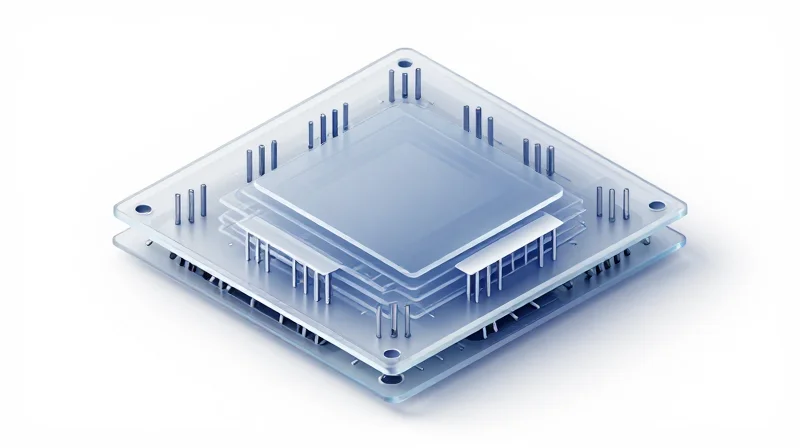
Strategic Implementation of Blind, Buried, and Microvias
In high-density multilayer boards (10–32 layers), standard through-hole vias consume excessive routing area and create unnecessary signal stubs. Utilizing blind, buried, and microvias is essential for escaping high-pin-count BGA components and maintaining signal integrity. For designs exceeding 14 layers, laser-drilled microvias (typically 0.10mm to 0.15mm in diameter) are mandatory to facilitate high-density routing.
Design Rules for Laser-Drilled Microvias
| Parameter | Recommended Standard | High-Reliability Constraint |
|---|---|---|
| Max Aspect Ratio | 1:1 | 0.75:1 |
| Pad-to-Via Clearance | 75um | 100um |
| Minimum Capture Pad | Via Diameter + 100um | Via Diameter + 150um |
To ensure reliable plating in these high-aspect-ratio holes, the via depth must not exceed the diameter in a 1:1 ratio. Exceeding this limit leads to insufficient copper deposition at the base, risking fatigue failure during thermal cycling. Buried vias connecting internal layer pairs must be staggered to maintain core structural integrity and prevent stress concentration points.
Via-in-Pad and BGA Escape Routing
- How do you handle BGA escape under high-density requirements?
Utilize microvias directly in the BGA pad, followed by a copper plating and cap process (IPC-4761 Type VII) to prevent solder wicking and ensure flat surface mounting. - What is the primary risk of buried vias in 32-layer boards?
The primary risk is dielectric thickness variation; ensure the stackup is symmetrical to prevent localized Z-axis expansion which can shear the buried via barrels. - Should I use staggered or stacked microvias?
Staggered vias are preferred for reliability. Stacked vias require specialized copper-filled plating processes to prevent structural voids and are only recommended when layer-count density prohibits any other routing strategy.
Optimizing Signal Integrity Through DFM

Managing Reference Plane Continuity
In boards ranging from 10 to 32 layers, signal integrity is primarily governed by the quality of the reference return path. Any discontinuity in a reference plane—caused by excessive antipad clearance in high-density via breakouts or slotting for thermal relief—forces return currents to take indirect paths. This significantly increases loop inductance, leading to heightened crosstalk and radiated EMI. Designers must prioritize solid, contiguous reference planes directly adjacent to high-speed signal layers, ensuring that the return path remains tightly coupled to the signal trace across all transitions.
Via Transition Strategies and Signal Integrity
As layer counts increase, signal vias often become the primary source of impedance mismatches. To minimize parasitic capacitance and inductance, implement the following DFM strategies for signal transitions:
- Stitching Vias
Place ground stitching vias in immediate proximity to signal via transitions to maintain a controlled return path loop as the signal jumps between layers. - Back-drilling
Remove excess via stubs in high-speed nets to prevent signal reflections and resonance, which are particularly damaging at frequencies exceeding 5 Gbps. - Antipad Optimization
Adjust antipad sizes on power and ground planes to maintain impedance continuity, balancing the need for physical clearance with the requirement for minimal parasitic capacitance.
Comparison of Crosstalk Mitigation Techniques
| Technique | Impact on Crosstalk | Manufacturing Complexity |
|---|---|---|
| Increased Trace Separation | High | Low |
| Guard Traces | Moderate | Medium |
| Reference Plane Shielding | Very High | Low |
| Differential Pair Tight Coupling | High | Low |
Critical DFM Considerations
To ensure reliable high-speed performance in dense multilayer assemblies, prioritize the synchronization of stackup design with your manufacturer’s registration capabilities. Misalignment between signal layers and their adjacent reference planes can introduce significant impedance deviations. Always verify that the dielectric constant (Dk) and dissipation factor (Df) are stable across the frequency range of interest, and avoid routing high-speed traces over plane splits at all costs.
Precision Alignment and Registration Challenges
Understanding Registration Tolerance and Material Dynamics
In boards ranging from 10 to 32 layers, the cumulative error from drilling and pressing can lead to registration failure. Registration is not merely a mechanical alignment issue; it is a materials science challenge driven by laminate movement during the multi-cycle lamination process. Thermal expansion, resin flow, and the inherent anisotropy of glass-reinforced fibers create micro-variations that propagate through the board stack-up, potentially shifting internal layers beyond the acceptable drill-capture threshold.
Managing Dimensional Instability
| Challenge Factor | Impact on Registration | Mitigation Strategy |
|---|---|---|
| Material Anisotropy | Differential expansion of fibers | Use of low-CTE, spread-glass materials |
| Thermal Cycle Count | Accumulated layer displacement | Sequential lamination protocols |
| Panel Size Effects | Edge-to-center scaling variance | Balanced copper distribution density |
DFM Strategies for Enhanced Registration
Design engineers must shift from standard clearance rules to manufacturing-aware designs that account for layer drift. By increasing the annular ring size on critical internal signal layers and implementing non-functional pad removal only when strictly necessary for impedance control, designers can improve the yield of boards with high layer counts.
- How does copper balance affect registration?
Unbalanced copper distribution causes localized heating differences during lamination, leading to uneven resin flow and layer shifting. Always maintain a balanced stack-up with symmetry in copper weight and distribution across the vertical axis. - What is the recommended approach for via-in-pad registration?
When utilizing via-in-pad technology for high-density BGA escapes, ensure the design incorporates a registration tolerance buffer of at least 3-5 mils beyond the standard drill diameter to account for mechanical registration limits of the drilling machine.
Ultimately, collaborating with the fabricator regarding their specific registration tolerance capabilities—typically measured in microns for high-layer-count builds—is essential. Defining the 'worst-case' layer-to-layer movement allows the design software to apply realistic keep-out zones during the CAD phase.
Thermal Management for Power-Hungry Designs

Strategic Thermal Dissipation in High-Density Stacks
As layer counts climb to 32, thermal management transitions from a cooling requirement to a primary structural design challenge. In high-density interconnects, the limited surface area demands that the PCB internal structure acts as a heat spreader. By utilizing internal ground planes as thermal sinks and incorporating high-density via stitching, designers can successfully conduct heat away from active semiconductor junctions and into the board substrate.
Copper Utilization and Via Arrays
To maximize thermal performance, designers must prioritize copper pours on internal layers. While signal layers often require density, maintaining consistent ground-plane coverage directly beneath high-power components provides a critical thermal mass. Furthermore, thermal via arrays should be positioned in a grid pattern directly under the component thermal pad, ensuring they connect to at least two internal solid copper planes to facilitate heat distribution.
| Technique | Thermal Benefit | DFM Consideration |
|---|---|---|
| Solid Copper Pours | High lateral heat spreading | Ensure balance to prevent board warp |
| Thermal Via Arrays | Low vertical resistance | Plugging/capping to prevent solder wicking |
| Thermal Relief Patterns | Controlled soldering heat | Optimize spoke width for current capacity |
Design Best Practices for Thermal Relief
- How do I balance thermal relief with current requirements?
Increase the number of spokes in your thermal relief patterns to lower resistance, but keep in mind that too much copper can make hand-soldering or rework difficult. - Why is via filling necessary for thermal vias?
In high-density boards, open thermal vias can cause solder wicking, leading to insufficient solder joint volume. Use conductive or non-conductive epoxy fill with copper capping. - What is the impact of board thickness on heat?
Thicker boards (up to 32 layers) provide higher thermal mass, but the increased dielectric material between layers can act as an insulator; therefore, consistent vertical via stitching is essential for through-board conduction.
DFM Checklist for Throughput and Yield
Pre-Fabrication Design Integrity Checklist
Achieving high yields on complex multilayer boards requires a systematic verification process before the data reaches the shop floor. By standardizing your design verification against specific manufacturing constraints, you significantly reduce the risk of board-level defects and costly engineering queries.
- Aspect Ratio Validation
Ensure via drilling depth-to-diameter ratios do not exceed 10:1 for high-density boards to prevent plating voids or barrel cracking during the thermal stress of reflow. - Copper Balancing
Maintain uniform copper distribution across all layers to minimize internal stresses, preventing board warp or bow during lamination cycles. - Annular Ring Compliance
Verify that your minimum annular ring specifications account for drill wander and registration tolerances, especially for inner layer pads in 20+ layer stacks. - Stack-up Symmetry
Implement symmetrical dielectric thickness and copper weight distribution to provide structural stability and controlled impedance across the entire board surface.
Manufacturing Constraint Comparison
| Feature | Standard Design (10-16 Layers) | Advanced Design (18-32 Layers) |
|---|---|---|
| Min Line/Space | 3.0 / 3.0 mil | 2.0 / 2.0 mil |
| Via Pad Diameter | 0.010 inch | 0.008 inch |
| Registration Tolerance | +/- 0.003 inch | +/- 0.0015 inch |
| Aspect Ratio | 8:1 | 12:1 (Laser microvias) |
Common DFM Pitfalls and Solutions
- Why do my high-layer boards exhibit excessive warpage?
This is typically caused by unbalanced copper distribution or asymmetric material construction in the stack-up. Ensure that every layer pair has a mirrored counterpart in terms of copper volume. - How can I improve drill accuracy for thin traces?
Transition to laser-drilled microvias for inter-layer connections in high-density regions, which reduces the reliance on large mechanical drills that introduce registration inaccuracies. - What is the impact of surface finish on yield?
For 20+ layer boards, flat finishes like ENIG or ENEPIG are critical to ensure coplanarity during high-speed component assembly, preventing solder joint bridging on fine-pitch pads.
Navigating the design of 10 to 32 layer PCBs is a complex process that demands technical precision and close collaboration with your fabrication partner. By adhering to these DFM best practices, you can effectively reduce prototyping iterations and accelerate your time-to-market. Ready to optimize your next high-density design? Contact our engineering team today for a comprehensive DFM review of your project files.
