
As industrial edge computing pushes the boundaries of performance in smaller form factors, traditional PCB design methods no longer suffice. Achieving signal integrity in high-density interconnect (HDI) boards requires a fundamental shift in how we approach layer stackups and manufacturing constraints. This guide provides the authoritative framework needed to navigate complex routing challenges and ensure your designs are production-ready from day one.
The Evolution of HDI in Edge Computing
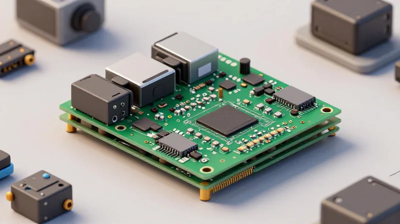
From Standard Manufacturing to HDI Architecture
In traditional PCB design, through-hole vias and standard trace routing were sufficient for industrial systems with larger form factors. However, the surge in edge computing demand—characterized by space-constrained enclosures, high-speed data processing, and complex silicon integration—has rendered these legacy methods obsolete. HDI technology utilizes microvias, blind vias, and buried vias to increase component density without bloating the board dimensions, effectively enabling complex multi-processor architectures to fit into compact edge nodes.
Comparison of Standard vs. HDI PCB Fabrication
| Feature | Standard PCB | HDI PCB |
|---|---|---|
| Via Technology | Through-hole only | Microvias, Blind, Buried |
| Trace/Space | Typically > 5 mil | Typically < 3 mil |
| Component Density | Low to Moderate | High to Ultra-High |
| Signal Integrity | Moderate | Excellent (Lower Latency) |
Strategic Drivers for Industrial Edge Adoption
The evolution of HDI is not merely a push for smaller boards; it is a fundamental shift in signal management. By reducing the physical path distance between the CPU, memory, and sensors, designers can significantly lower parasitic inductance and capacitance. This is critical for industrial applications operating in high-interference environments, where signal noise can compromise machine learning inference and real-time control loops.
- Why does miniaturization require HDI?
Smaller footprints limit real estate for routing; HDI allows the use of stacked microvias that save board area and provide shorter signal paths. - How does HDI improve industrial reliability?
By minimizing trace lengths and utilizing more efficient thermal dissipation paths, HDI boards offer better signal integrity and lower thermal stress during 24/7 industrial operation. - Is HDI adoption more expensive?
While unit fabrication costs are higher due to laser drilling and sophisticated plating requirements, the reduction in PCB layers and system-level miniaturization often yields a lower total cost of ownership for compact hardware.
Strategic Layer Stackup Planning
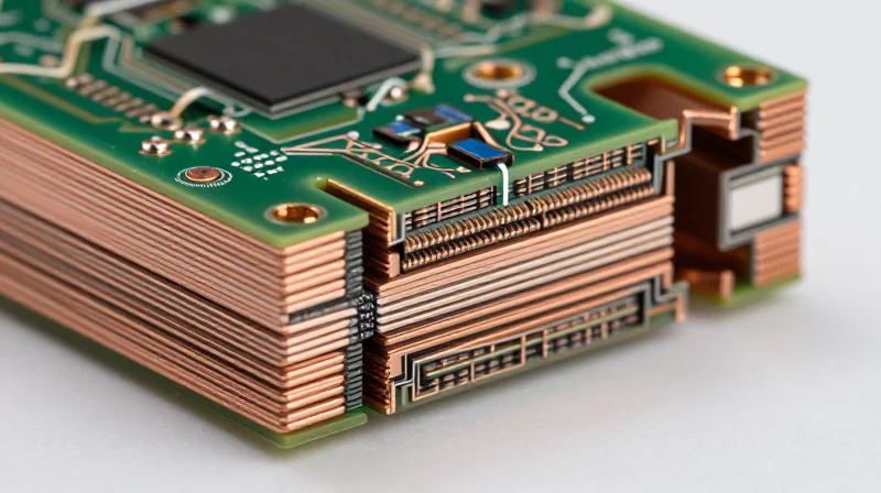
Balancing Density, Impedance, and Thermal Performance
Effective layer stackup design is the bedrock of HDI success. In compact industrial edge devices, the challenge is minimizing layer counts to manage cost while increasing via density to accommodate high-pin-count BGA components. Engineers must prioritize a balanced construction to prevent mechanical warpage, ensuring that the copper distribution is symmetric across the neutral axis of the board.
| Design Priority | Stackup Consideration | Recommended Strategy |
|---|---|---|
| Signal Integrity | Impedance Control | Ensure tight coupling between signal and reference planes using thin dielectrics. |
| Power Delivery | Plane Capacitance | Utilize ultra-thin core materials to maximize inter-plane capacitance for high-speed noise suppression. |
| Thermal Flow | Heat Spreading | Integrate solid copper planes tied to thermal vias directly under high-heat components. |
Optimizing via Structures for HDI
The transition from through-hole vias to microvias significantly reduces the footprint required for fan-outs. Utilizing 'Any-Layer' HDI (ELIC) technology allows for unrestricted routing between layers, effectively reducing board size by 30-40%. However, excessive via stacking can lead to reliability issues; it is recommended to utilize staggered vias wherever possible to mitigate stress concentration during thermal cycling.
Strategic Stackup FAQ
- How does layer count impact thermal management?
Increased layer counts generally improve thermal dissipation by allowing for dedicated internal ground planes that act as heat spreaders, provided they are effectively stitched with thermal vias. - Is impedance control achievable on ultra-thin HDI dielectrics?
Yes, but it requires precise control of trace width and copper thickness, as the proximity to reference planes on thin cores significantly lowers the trace impedance, necessitating narrower trace widths. - When should I choose stacked vs. staggered microvias?
Stacked vias are preferred for space-constrained signal routing under dense BGAs, whereas staggered vias offer superior structural reliability in environments subject to high vibration and extreme thermal shock.
Mastering Microvia Geometry and Types
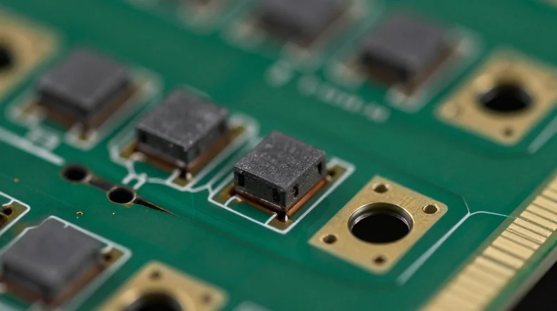
Defining Microvia Geometry and Aspect Ratios
In HDI design, microvias are laser-drilled structures typically defined as having a diameter of 150 microns or less. The most critical geometric constraint is the aspect ratio (depth-to-diameter), which directly dictates the success of the copper plating process. For robust reliability in industrial edge hardware, designers must maintain an aspect ratio of 0.75:1 or lower to ensure uniform dielectric coverage and avoid voiding within the via barrel.
Comparative Analysis: Blind vs. Buried Vias
| Via Type | Fabrication Complexity | Best Use Case | Primary Design Constraint |
|---|---|---|---|
| Blind Microvia | Moderate | Outer layer connection to inner layer | Sequential lamination alignment |
| Buried Microvia | High | Internal routing/high-density signal transitions | Layer count and thermal expansion match |
| Stacked Microvia | Very High | Maximum density vertical signal paths | Copper plating fill uniformity |
Reliability and DFM Best Practices
Reliability concerns in microvias often stem from CTE (Coefficient of Thermal Expansion) mismatches between the copper plating and the laminate substrate. To mitigate these risks, avoid 'staggered-only' designs where possible, as stacked microvias—when properly filled—offer a more uniform structural profile. Always ensure the landing pad is at least 50 microns larger than the via diameter to account for laser drill tolerances.
- Why is the aspect ratio of 0.75:1 recommended?
Lower aspect ratios reduce the difficulty of copper plating the via walls, preventing 'dog-boning' and ensuring a robust connection between the laser-drilled hole and the internal capture pad. - Should I use filled or unplugged microvias?
For high-density BGA packages, microvias should always be filled with conductive or non-conductive epoxy and capped with copper to allow for 'via-in-pad' designs, which significantly improves signal integrity. - How does surface finish affect microvia reliability?
Processes like ENIG (Electroless Nickel Immersion Gold) can introduce brittle intermetallic layers; ensure that your microvia capture pads are sized sufficiently to absorb thermal stresses during the reflow process.
Design for Manufacturing (DFM) Core Rules
Critical Geometry and Spacing Constraints
In HDI designs, the margin for error in etching and registration is significantly reduced. Precise control over pad-to-trace spacing and annular ring integrity is the primary defense against internal layer shorts and pad cratering during assembly.
| Feature | Typical HDI Minimum | Fabrication Concern |
|---|---|---|
| Pad-to-Trace Spacing | 2.0 - 3.0 mil | Etch factor / Shorting |
| Annular Ring | 1.5 - 2.0 mil | Drill breakout |
| Copper Pour Clearance | 5.0 mil | Solder bridging |
Copper Balancing and Thermal Integrity
Asymmetric copper distribution is the leading cause of board warp and twist during lamination. For HDI boards, maintaining copper balance across the Z-axis is not merely a structural requirement but a functional one for impedance control and heat dissipation in edge computing enclosures.
Frequently Asked DFM Questions
- Why is the aspect ratio of microvias critical for reliability?
A high aspect ratio (typically >0.75:1) makes consistent copper plating within the microvia barrel difficult, leading to thermal expansion stresses and crack propagation during reflow cycles. - How does copper balance impact the final board thickness?
Poor balance leads to uneven resin flow during the lamination cycle, which forces non-uniform dielectric thicknesses, causing impedance deviations across the PCB. - Can I use standard solder mask tolerances for HDI?
No, standard tolerances are insufficient. HDI requires defined registration (LDI-Direct Imaging) to ensure the solder mask opening does not encroach upon fine-pitch BGA pads, which would otherwise result in 'solder mask defined' errors or poor wetting.
Mitigating Signal Interference in Dense Layouts

Minimizing Crosstalk in High-Density Environments
In compact industrial edge hardware, crosstalk becomes the primary bottleneck as routing density increases. To mitigate coupling, designers must prioritize trace geometry and the proximity of return paths. Maintaining a strict 3W rule (trace-to-trace spacing at least three times the trace width) is the baseline, but in HDI designs, this often fails due to spatial constraints. Consequently, transitioning to differential pair routing with tight coupling and minimizing parallel trace runs between layers are essential defensive measures.
| Mitigation Technique | Mechanism | Implementation Priority |
|---|---|---|
| Differential Signaling | Phase alignment and tight coupling | High |
| Orthogonal Routing | Reducing parallel coupling capacitance | High |
| Vertical Isolation | Shielding via intermediate ground planes | Critical |
Effective Ground Plane Segmentation
Ground plane segmentation is a delicate balance between noise isolation and return path continuity. In HDI boards, cutting planes to separate analog and digital domains often inadvertently creates loop areas that act as antennas. Instead of physical fragmentation, use solid reference planes and restrict signal paths to dedicated zones. When segmentation is unavoidable for high-precision sensors, use a single-point connection (bridge) to minimize loop inductance.
Design Best Practices FAQ
- How do microvias influence EMI in dense boards?
Microvias reduce the size of current loops compared to through-hole vias, significantly lowering parasitic inductance and improving EMI performance. - Is it safe to route signals over plane splits?
Never route high-speed signals over a plane split; this forces the return current to take a longer path, causing massive impedance discontinuities and electromagnetic radiation. - What is the role of stitching vias in crosstalk reduction?
Ground stitching vias along the perimeter of high-speed zones create a Faraday cage-like structure, containing fields and preventing lateral crosstalk between high-density routing channels.
Advanced Laser Drilling Technologies
Precision Laser Ablation in Modern HDI PCBs
Modern industrial edge hardware demands microvias with extreme accuracy and clean sidewall integrity. Laser ablation—specifically utilizing CO2 and UV lasers—allows for the creation of vias that exceed the capabilities of traditional mechanical drilling, especially when dealing with ultra-thin dielectric layers and blind via structures.
The choice between CO2 and UV lasers often dictates the final quality of the hole wall and the potential for residual debris, known as 'smear.' Proper parameter optimization is critical to ensure reliable plating during the subsequent metallization process.
| Laser Technology | Primary Application | Precision Level | Surface Finish |
|---|---|---|---|
| CO2 Laser | Dielectric removal (bulk) | Medium | Moderate |
| UV Laser (YAG) | Micro-via definition | Ultra-high | Excellent |
| Hybrid (CO2 + UV) | Complex material stacks | High | Superior |
Optimizing Laser Drilling Parameters
- How does laser pulse width impact via reliability?
Shorter pulse widths reduce the Heat Affected Zone (HAZ), preventing thermal stress and micro-cracking in the surrounding dielectric, which is essential for long-term reliability in edge devices. - Why is copper-to-dielectric selectivity important?
High selectivity allows the laser to ablate the dielectric without damaging the copper capture pads, ensuring the integrity of the electrical connection after plating. - What role does debris removal play in plating?
Laser drilling creates carbonized residue. If not removed via chemical desmear or plasma cleaning, it creates voids in the copper plating, leading to intermittent signal failures in high-vibration industrial environments.
Engineers must specify 'laser-direct' drill files that account for the beam diameter and the specific material stack-up. Failing to provide accurate ablation data can lead to tapered holes, which increase the risk of plating fatigue under the thermal cycling conditions common in edge computing hardware.
Thermal Management for Compact Assemblies
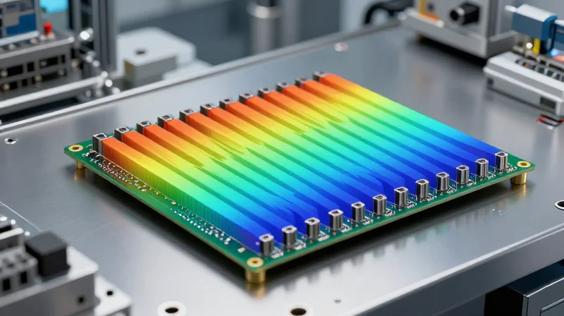
Thermal Management Strategies for HDI Assemblies
Effective heat dissipation in high-density interconnect (HDI) designs requires a holistic approach that moves heat from high-power silicon components through the PCB substrate into the chassis or heat sink. Because HDI boards lack significant surface area for convection, designers must leverage the PCB itself as a thermal conduit.
Optimizing Thermal Via Arrays
Thermal vias serve as the primary bridge between surface-mounted power components and internal ground planes. To maximize efficiency, utilize a dense array of small-diameter through-hole vias directly beneath thermal pads. When using via-in-pad technology, these must be copper-plugged and capped to prevent solder wicking and ensure structural integrity.
| Parameter | Recommended Practice | Performance Impact |
|---|---|---|
| Via Diameter | 0.2mm to 0.3mm | Maximizes surface-to-volume copper ratio |
| Via Plating | 25µm minimum | Improves thermal conductivity through the barrel |
| Array Spacing | 1.0mm to 1.2mm pitch | Balances thermal mass with structural stability |
Material Selection: The Role of High-Tg Dielectrics
In industrial environments where edge computing units experience significant temperature fluctuations, standard FR-4 materials are often insufficient. Using materials with a high Glass Transition Temperature (Tg > 170°C) is mandatory to prevent board delamination and pad lifting caused by Z-axis expansion during thermal cycling.
- Why is thermal conductivity of the substrate important?
A substrate with higher thermal conductivity helps spread heat laterally across the board surface, reducing localized hotspots that would otherwise lead to early component failure. - How does copper balance impact thermal management?
Proper copper balancing is not only for warpage prevention; it creates a uniform thermal expansion profile, ensuring that the board does not experience mechanical stress concentrations during operation. - When should metal-core PCBs be considered?
If thermal via arrays alone cannot dissipate the heat flux from high-performance CPUs or FPGAs, transition to a metal-core (IMS) substrate or localized copper coins to provide a low-resistance path to the heat sink.
Validating HDI Designs Before Fabrication
The Role of Rigorous Design Rule Checking (DRC)
DRC is the primary gatekeeper in the transition from digital design to physical manufacturing. For HDI boards featuring microvias, blind vias, and fine-pitch BGA footprints, standard design rules are insufficient. Designers must implement high-fidelity constraint sets that specifically target the manufacturing limits of the chosen process, such as aspect ratios for laser-drilled holes and annular ring clearances for stacked via structures.
Pre-Production Collaboration with Fabrication Partners
Engagement with your fabricator should occur long before final sign-off. Early DFM reviews allow fabrication engineers to assess the stack-up and routing complexity against their specific process window. This collaboration helps identify potential yield killers—such as uneven plating distribution in tight trace gaps or thermal expansion mismatches—before they reach the shop floor.
| Validation Step | Primary Goal | Failure Mode Addressed |
|---|---|---|
| Pre-Layout DRC | Set technology constraints | Violation of fabricator minimums |
| Stack-up Analysis | Ensure impedance/thermal control | Signal integrity and warpage |
| Panelization Review | Optimize material utilization | Unnecessary cost or panel stress |
| CAM Check | Verify actual tooling output | File misinterpretation or scaling errors |
Key Considerations for HDI Validation
- Why is stacked-via verification critical?
Stacked vias introduce significant stress points; verifying copper fill and plating thickness is vital to prevent barrel cracking during reflow. - How does aspect ratio affect HDI yield?
Higher laser drilling aspect ratios increase the risk of poor plating deposition at the base of the microvia, leading to intermittent open circuits. - What should be included in a DFM package?
Include ODB++ or IPC-2581 data, specific stack-up requirements, controlled impedance tables, and clear documentation regarding non-standard via-in-pad treatments.
Ultimately, the transition to production should be treated as a partnership. By automating DRC checks within the CAD environment and verifying files against the manufacturer's specific DFM guidelines, designers can avoid costly prototype iterations and ensure high-reliability performance in the field.
Successfully implementing HDI technology is the bridge between conceptual design and market-leading hardware. By adhering to these rigorous DFM standards, you can minimize board failure, reduce iteration cycles, and ensure optimal performance in the field. Ready to optimize your board for high-density production? Contact our engineering team today for a comprehensive design review.
