
In the fast-evolving landscape of smart grid infrastructure, failure is not an option. Metering electronics must withstand harsh environments while maintaining absolute data integrity over decades. This guide explores the intersection of precision PCB layout and advanced DFM practices that ensure your hardware remains resilient, accurate, and manufactured to the highest industry standards.
The Critical Importance of DFM in Metering Applications
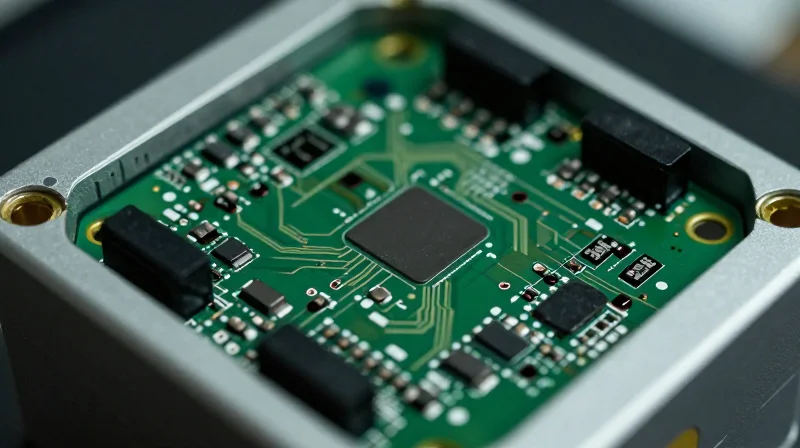
The Strategic Value of DFM in Smart Grid Infrastructure
In the context of smart grid metering, a printed circuit board (PCB) is not merely a component; it is a critical asset expected to perform flawlessly under harsh environmental conditions for over a decade. DFM is the practice of optimizing the design process to ensure the board is manufacturable, reliable, and cost-effective from the outset, mitigating the risks of field failures that could compromise grid data integrity or energy billing accuracy.
Mitigating Risks Through Proactive Design
High-reliability metering demands rigorous attention to thermal management, signal integrity, and structural robustness. Integrating DFM rules early prevents common manufacturing defects such as acid traps, slivers, and uneven copper distribution, which can lead to latent failures after years of service in outdoor environments.
| Design Factor | Manufacturing Impact | Reliability Outcome |
|---|---|---|
| Trace Geometry | Uniform plating distribution | Prevents localized heating and opens |
| Via Placement | Stress reduction during reflow | Eliminates barrel cracking in cycles |
| Component Spacing | Assembly efficiency | Reduces solder bridging risks |
- Why is DFM critical for smart meters?
Smart meters operate in non-climate-controlled environments; DFM ensures the board can withstand extreme thermal cycling and moisture without degrading. - Does DFM improve production speed?
Yes, by eliminating design bottlenecks and manufacturability issues, DFM reduces the need for costly engineering changes during the production ramp-up phase. - How does DFM affect long-term maintenance?
Boards designed with DFM principles exhibit lower Field Failure Rates (FFR), significantly reducing the operational expense associated with meter recalls and field replacements.
Advanced Signal Integrity Strategies for Mixed-Signal Boards

Strategies for Mixed-Signal Isolation
Achieving signal integrity in smart grid meters requires a strategic physical partition between the noisy digital switching elements—such as microcontrollers and communication transceivers—and the sensitive high-precision analog front-end (AFE) components. By implementing rigorous ground plane segmentation or sophisticated star-grounding topologies, designers can prevent return currents from high-speed digital loops from traversing sensitive measurement paths, thereby preserving the signal-to-noise ratio essential for billing accuracy.
Design Best Practices Comparison
| Strategy | Primary Benefit | Implementation Challenge |
|---|---|---|
| Split Ground Planes | Hard noise isolation | Risk of EMI if bridged improperly |
| Star Grounding | Common reference point | Routing complexity at high frequencies |
| Differential Signaling | Common-mode noise rejection | Requires strict trace matching |
Frequently Asked Questions on Signal Integrity
- How does digital noise influence measurement accuracy?
Digital switching transients create high-frequency ripples on power rails and ground planes, which can capacitively couple into the analog measurement trace, manifesting as jitter or DC offset in current and voltage readings. - Is a split ground plane always recommended?
Not necessarily; while splitting planes provides excellent isolation, improper bridging over the gap can create massive return current loops that act as highly efficient antennas, potentially failing EMC compliance standards. - What is the best way to handle signal vias?
Minimize the number of via transitions for sensitive signals. If transitions are necessary, ensure that a stitching via is placed immediately adjacent to the signal via to provide a low-impedance return path.
Optimal Component Placement and Routing Patterns
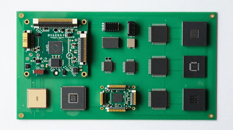
Component Placement Strategy for Thermal and Electrical Stability
Effective placement is governed by the need to isolate high-energy switching components from precision metrology front-ends. By clustering power conversion stages away from sensitive analog-to-digital converters, designers can minimize electromagnetic interference (EMI). Furthermore, placing high-power components near the board edges or over thermal vias ensures efficient heat dissipation, preventing localized hotspots that could accelerate component aging.
Minimizing Crosstalk in Mixed-Signal Routing
Routing patterns must prioritize trace impedance control and signal isolation. To prevent crosstalk between low-voltage sensing signals and high-speed communications, designers should adopt a strict 'keep-out' zoning strategy. Utilizing differential pair routing for clock and communication lines further improves noise immunity in harsh industrial environments.
| Design Factor | Recommended Practice | Key Benefit |
|---|---|---|
| High-Power Placement | Near board edge/large copper pour | Improved heat dissipation |
| Analog Routing | Keep length minimal/shielded | Reduced noise floor |
| Crosstalk Control | Increase trace spacing (3W rule) | Decreased inductive coupling |
Frequently Asked Questions
- How does board density affect manufacturing yields?
Excessive component density can lead to solder bridging and increased risk of thermal damage during reflow; maintaining appropriate clearance is vital for reliable assembly. - Are there specific routing rules for Smart Grid metering?
Yes, maintaining galvanic isolation distances is critical, as is ensuring that high-voltage traces remain separated from low-voltage logic to meet strict safety and certification standards.
Surface Finish Selection for Long-Term Reliability
For high-reliability smart grid hardware, the surface finish acts as the final barrier between the copper circuitry and environmental contaminants. The choice between finishes like Electroless Nickel Immersion Gold (ENIG) and Immersion Silver (ImAg) dictates not only immediate manufacturing yield but also long-term resistance to oxidation, corrosion, and mechanical stress during thermal cycling.
Surface Finish Comparative Analysis
| Finish Type | Solderability | Environmental Resistance | Best Application |
|---|---|---|---|
| ENIG | Excellent | High (Excellent Corrosion Resistance) | High-Density BGAs & Long-Life Meters |
| Immersion Silver | Excellent | Moderate (Requires Care) | Cost-Sensitive High-Reliability Designs |
| HASL (Lead-Free) | Good | Moderate | General Purpose Industrial Controls |
Key Considerations for Smart Grid Environments
Smart grid meters are often installed in outdoor enclosures where they face extreme humidity and fluctuating temperatures for over a decade. ENIG remains the industry standard for these applications due to the nickel layer providing a diffusion barrier and the gold layer ensuring superior shelf life. However, designers must mitigate 'black pad' risks by ensuring robust plating control during the fabrication process.
Frequently Asked Questions
- Why is ENIG preferred for long-term field deployment?
ENIG offers excellent oxidation resistance and a flat surface plane which is vital for fine-pitch component mounting, ensuring minimal mechanical stress on solder joints during temperature shifts. - What are the primary risks associated with Immersion Silver?
Immersion Silver is prone to tarnish if exposed to sulfur-bearing environments and has a shorter shelf life, requiring strict handling protocols in the assembly facility to maintain solderability. - How does surface finish affect thermal cycling reliability?
The mechanical robustness of the intermetallic compound (IMC) layer formed during soldering is heavily dependent on the purity and type of the finish; choices like ENIG provide more stable metallurgical interfaces under continuous thermal stress.
Mitigating Electromagnetic Interference (EMI) in Smart Meters
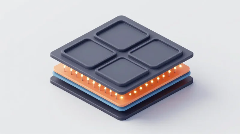
Advanced Grounding Strategies for EMI Reduction
For high-reliability smart meters, a dedicated ground plane is non-negotiable. To achieve superior EMI performance, engineers must implement a solid reference plane to provide the lowest impedance path for return currents. By employing a multi-layer stack-up where signal layers are closely coupled to a reference plane, designers can drastically reduce loop area and radiated emissions.
Shielding and Board-Level Containment
Board-level shielding serves as the first line of defense against both external interference and internal coupling between high-frequency communication modules and sensitive measurement circuitry. Implementing Faraday cages around RF front-ends is essential for compliance with standards such as FCC Part 15 and CISPR 32.
| Shielding Method | Primary Application | EMI Benefit |
|---|---|---|
| Formed Metal Cans | RF/Wireless Modules | High-attenuation of radiated fields |
| Via Fencing | Board Edge/Traces | Reduces edge radiation and crosstalk |
| Grounded Heat Sinks | High-Power Processors | Combines thermal management with RF containment |
Common EMI Design Considerations
- How do via fences assist with EMI?
Stitching vias along the PCB perimeter creates a low-impedance boundary that prevents electromagnetic waves from propagating along the board edges, effectively acting as a containment wall. - Why should analog and digital grounds be managed carefully?
While physically distinct in some topologies, they must remain at the same potential. Implementing a single-point connection or a bridge prevents high-frequency noise from the digital processing block from polluting the analog metrology measurements. - What role does stack-up play in compliance?
A well-designed stack-up minimizes the distance between the signal layer and the return plane. This proximity minimizes the inductive loop area, which is the primary source of common-mode radiation.
Advanced Environmental Protection: Conformal Coating and Potting
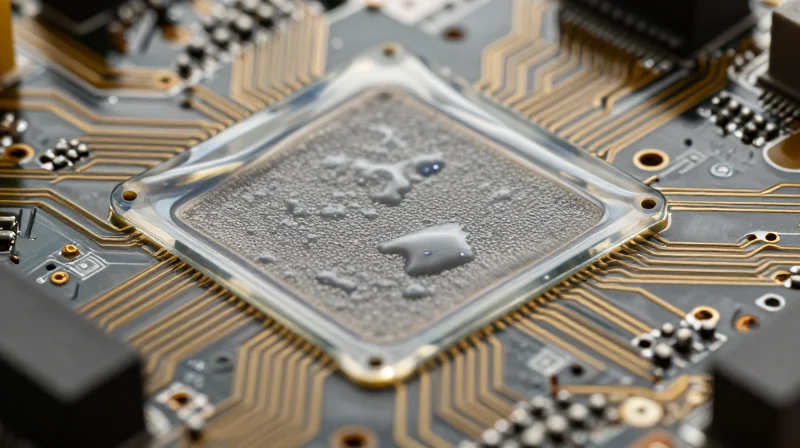
Conformal Coating vs. Potting for Smart Meter Reliability
Smart grid meters frequently operate in extreme outdoor environments, necessitating robust barriers against moisture, condensation, salt spray, and particulate contaminants. Selecting the appropriate protection method requires a trade-off analysis between weight, accessibility for rework, and the degree of environmental isolation required.
| Feature | Conformal Coating | Potting Compound |
|---|---|---|
| Application | Thin protective layer | Encapsulation of assembly |
| Environmental Seal | Good (Moisture/Dust) | Excellent (Hermetic-like) |
| Repairability | Possible with solvent | Very difficult |
| Weight/Volume | Minimal impact | Significant increase |
Key Environmental Protection Considerations
- Why is material selection critical for smart meters?
Materials must possess high dielectric strength, low moisture absorption rates, and stable performance across wide temperature ranges (-40°C to +85°C) to prevent leakage currents and signal degradation. - How does surface tension impact conformal coating DFM?
Designers must ensure proper clearance around tall components and connectors to prevent 'wicking,' where liquid coating migrates into electrical contacts via capillary action during application. - When is potting strictly required?
Potting is recommended for high-voltage sections of the smart meter where dielectric breakdown risk is high, or for units deployed in high-salinity coastal regions where thin coatings may fail due to oxidation.
Implementation Best Practices
To ensure long-term field success, masking strategies must be precisely defined during the DFM phase. Incompatible materials or poor surface preparation—such as residual flux or ionic contamination—will cause delamination and failure under thermal cycling. Utilize automated dispensing systems to maintain consistent thickness across high-density component arrays, ensuring total coverage of solder joints while avoiding stress-sensitive components like crystals or high-wattage inductors that require specialized stress-relief compounds.
Rigorous Testing and Quality Assurance Protocols
Establishing Quality Gates for Smart Grid Reliability
Smart grid infrastructure demands an uncompromising level of hardware reliability, as meters often operate in uncontrolled outdoor environments for over a decade. Rigorous testing protocols serve as the final gate to intercept latent manufacturing defects, such as cold solder joints, microscopic shorts, or component misplacements that could lead to field failures. By implementing a multi-layered testing strategy, manufacturers can ensure that every PCB conforms to stringent performance specifications before deployment.
Comparative Analysis: ICT vs. Flying Probe
| Feature | In-Circuit Testing (ICT) | Flying Probe |
|---|---|---|
| Setup Cost | High (Custom Fixtures Required) | Low (Fixtureless) |
| Test Speed | Very Fast (High Volume) | Slower (Prototyping/Low Volume) |
| Access Requirements | Test points required on all nets | Accessible via surface pads/vias |
| Best Application | Mass production smart meters | Low-volume runs and R&D |
Testing Strategy FAQ
- Why is ICT still considered the gold standard for high-volume metering?
ICT offers unparalleled speed and fault coverage, allowing for comprehensive power-up tests and component-level verification in seconds, which is essential for scaling smart meter manufacturing. - How does Flying Probe assist in the DFM phase?
Flying probe testing is invaluable during the NPI (New Product Introduction) phase because it allows engineers to test complex board designs without the expensive design-and-build cycle of custom bed-of-nails fixtures. - What role does Boundary Scan (JTAG) play in these protocols?
For modern smart meters featuring complex ICs and FPGAs, Boundary Scan complements ICT by allowing internal testing of logic paths that are otherwise unreachable by physical probes, ensuring that internal connectivity is intact.
Manufacturers should integrate automated optical inspection (AOI) alongside electrical testing to detect visual defects that electrical tests might miss, such as solder bridges or incorrect component polarity. A synchronized approach—combining optical, flying probe, and ICT—creates a robust framework that minimizes field returns and maximizes grid uptime.
By integrating these DFM principles into your development lifecycle, you can significantly reduce failure rates and extend the operational life of your smart grid hardware. Whether you are scaling production or designing a next-gen prototype, our engineering team is here to assist. Contact us today for a comprehensive design review of your next high-reliability project.
