
As 5G networks push data rates into the millimeter-wave spectrum, the traditional margins for PCB error have effectively vanished. For hardware engineers and manufacturing leads, the challenge isn't just signal routing; it is ensuring that your design survives the rigorous demands of fabrication and high-thermal environments. This guide breaks down the critical Design-for-Manufacturing (DFM) rules necessary to achieve perfect signal integrity and manufacturing repeatability.
Understanding High-Frequency Signal Integrity Challenges

Fundamental Signal Integrity Degradation Mechanisms
At 5G frequencies, signal propagation is no longer governed by simple resistive paths but by complex electromagnetic field interactions. The primary challenges involve energy dissipation that scales non-linearly with frequency, necessitating precision in material selection and fabrication processes.
- Skin Effect
As frequency increases, current density migrates toward the outer surface of the copper trace. This reduction in effective cross-sectional area increases conductor resistance, leading to significant insertion loss. - Dielectric Loss (Tan δ)
The PCB substrate absorbs electromagnetic energy, converting it into heat. Selecting materials with an ultra-low dissipation factor is essential to maintaining signal amplitude over longer interconnect lengths. - Copper Surface Roughness
High-frequency currents flow along the peaks and valleys of the copper trace. If the profile is too rough, the effective path length increases, compounding insertion loss and introducing signal jitter.
Material Performance Comparison for High-Frequency PCBs
| Parameter | Standard FR-4 | High-Speed Laminate | PTFE/Ceramic |
|---|---|---|---|
| Dielectric Constant (Dk) | 4.4 - 4.8 | 3.2 - 3.8 | 2.1 - 3.0 |
| Dissipation Factor (Df) | 0.020 | 0.005 - 0.010 | < 0.002 |
| Best Application | Low-frequency logic | General 5G Infrastructure | RF Front-End/Antenna |
Mitigation Strategies via Design Rules
To mitigate these losses, DFM protocols must mandate the use of VLP (Very Low Profile) or HVLP (Hyper Very Low Profile) copper foils. Furthermore, trace geometry must be tightly controlled using impedance-matched modeling to prevent reflections that compound insertion loss signatures. By minimizing roughness at the copper-dielectric interface, designers can significantly lower the signal attenuation threshold, ensuring robust performance across the sub-6 GHz and mmWave spectrums.
Precision Impedance Control Strategies
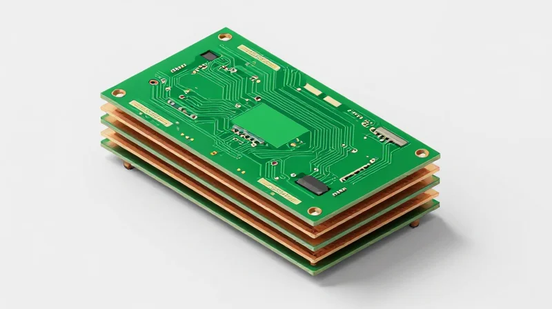
In 5G high-frequency applications, signal integrity is fundamentally tied to the consistency of characteristic impedance. Even minor deviations from the target impedance—typically 50 ohms single-ended or 100 ohms differential—cause reflections, jitter, and excessive return loss. Achieving ±5% tolerance requires a holistic approach encompassing precise etch factor compensation, controlled dielectric thickness, and advanced surface finish application.
Optimizing Trace Geometry and Etch Compensation
The chemical etching process inherently creates trapezoidal traces rather than perfectly rectangular ones. As trace pitch shrinks to accommodate high-density interconnects, the etch factor becomes the most critical variable. DFM rules must mandate a trace width compensation factor that accounts for copper weight and dielectric thickness variations.
| Parameter | Standard Tolerance | High-Frequency Requirement |
|---|---|---|
| Trace Width | ±10% | ±3% |
| Dielectric Thickness | ±10% | ±5% |
| Copper Roughness | Nominal | Low-Profile (VLP/HVLP) |
Critical DFM Best Practices
- How does copper surface roughness impact impedance?
Increased roughness increases signal path length and effective resistance at high frequencies due to the skin effect, which can lead to unpredictable impedance shifts and dielectric heating. - Why is material selection vital for impedance control?
Materials with a stable Dielectric Constant (Dk) across the frequency spectrum are required to prevent impedance drift as 5G signal frequencies fluctuate between 24GHz and 40GHz+. - What role do reference planes play?
Ensuring continuous, gap-free ground reference planes is mandatory to maintain a consistent return path and prevent electromagnetic radiation at board transitions.
Advanced Design Guidelines for Manufacturing
1. Utilize VLP (Very Low Profile) copper foils to minimize skin-effect impedance variance.
2. Apply a strict 1:1 etch factor ratio for critical differential pairs to maintain symmetry.
3. Implement blind/buried via structures to eliminate capacitive stubs that cause resonance.
4. Design symmetrical stack-ups to prevent board warpage during lamination, which ensures dielectric consistency.
Microvia Reliability in Multi-Layer Assemblies
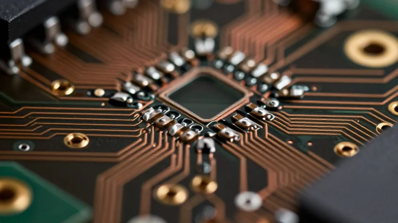
Microvia Reliability in Multi-Layer Assemblies
As 5G designs drive higher layer counts and finer pitch requirements, microvias become the most vulnerable points for structural failure. Barrel cracking and delamination often stem from mismatched Coefficient of Thermal Expansion (CTE) between the copper plating and the dielectric material. To mitigate these risks, designers must prioritize strict aspect ratio adherence and optimized plating thickness to ensure durability under thermal stress.
Design Guidelines for Microvia Longevity
| Parameter | Recommended Limit | Impact on Reliability |
|---|---|---|
| Aspect Ratio | Max 0.75:1 | Reduces plating stress during thermal cycling |
| Plating Thickness | Min 20-25µm | Prevents barrel cracking and brittle fractures |
| Pad-to-Via Annular Ring | Min 50µm | Ensures connectivity and alignment stability |
Common Failure Mitigation FAQ
- How does aspect ratio affect plating consistency?
Higher aspect ratios make it difficult for plating solutions to reach the bottom of the via, leading to thin copper walls that are prone to tensile failure under thermal expansion. - What is the primary cause of microvia delamination?
Delamination is frequently caused by insufficient curing of the resin system or contamination within the via hole prior to metallization, which prevents a strong mechanical bond. - Why is copper plating thickness critical for 5G?
In high-frequency applications, signal integrity depends on uniform cross-sections; inconsistent plating thickness alters impedance, while overly thin plating acts as a weak point for mechanical fatigue.
Engineers should specify stacked or staggered via structures based on the specific thermal profile of the end-use device. For 5G infrastructure equipment, staggered vias are generally preferred to distribute mechanical stress across multiple layers, thereby minimizing the potential for cumulative structural failure.
Mitigating Thermal Expansion and CTE Mismatch
Managing CTE Mismatch in High-Frequency Assemblies
Thermal expansion-induced stress is a primary failure vector in 5G high-frequency PCBs. Because 5G infrastructure often experiences significant power-cycling, the disparity in CTE between dielectric materials and copper conductors can lead to via barrel cracking, pad lifting, and delamination. To maintain signal integrity and mechanical stability, engineers must prioritize material selection that aligns the Z-axis CTE of the laminate with that of the plated through-holes.
Substrate Material Selection Criteria
Selecting a substrate for 5G applications requires balancing electrical performance (low Dk/Df) with mechanical robustness. Focus on materials with high Glass Transition Temperatures (Tg) and low CTE values in the Z-axis to prevent dimensional instability during reflow and high-frequency operation.
| Material Property | Target Metric | Impact on Reliability |
|---|---|---|
| Glass Transition (Tg) | > 180°C | Maintains structural rigidity during high thermal excursions. |
| Z-Axis CTE | < 3.0% (50-260°C) | Reduces stress on microvia barrels and interconnections. |
| Decomposition Temp (Td) | > 350°C | Prevents outgassing and delamination in lead-free assembly. |
Design Guidelines for Thermal Stability
- How can copper balancing mitigate thermal warping?
Implement symmetrical copper distribution across all layers to ensure uniform expansion rates, effectively preventing the PCB from bowing or twisting under high thermal loads. - Why is the Z-axis CTE critical for microvias?
During thermal cycling, the PCB dielectric expands faster than the copper via. If the CTE exceeds 3%, the resulting tensile stress often exceeds the elongation limits of the copper plating, leading to fracture. - What role does weave style play?
Utilize 'spread glass' or 'flat-weave' fabric architectures to provide more uniform dielectric constants and consistent thermal expansion properties across the board surface.
Advanced Copper Foil Selection for Insertion Loss Reduction
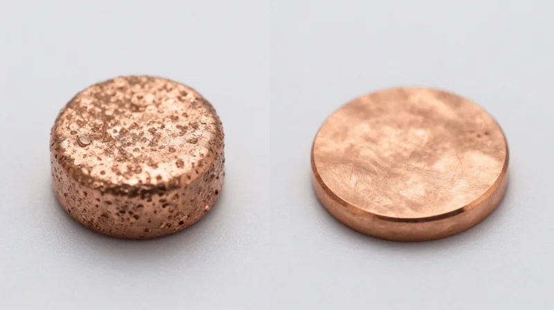
The Impact of Surface Roughness on Signal Integrity
At 5G frequencies exceeding 20GHz, the skin effect restricts current flow to a thin layer at the surface of the copper conductor. If the copper foil surface is rough, the effective path length of the signal increases significantly, leading to higher conductor loss. Utilizing low-profile and Very Low Profile (VLP) copper foils is a critical DFM strategy to maintain signal integrity by minimizing surface roughness and reducing the dissipation factor.
| Foil Type | Average Roughness (Rz) | Primary Application | Insertion Loss Impact |
|---|---|---|---|
| Standard Electro-Deposited (STD) | 4.0 - 6.0 µm | Low-frequency digital | High loss at >10GHz |
| Low Profile (LP) | 2.0 - 3.0 µm | High-speed digital | Moderate loss reduction |
| Very Low Profile (VLP) | 0.8 - 1.5 µm | 5G / mmWave RF | Minimal insertion loss |
| Hyper-Low Profile (HVLP) | < 0.8 µm | Advanced 5G infrastructure | Optimized signal integrity |
Material Selection Criteria and DFM Considerations
While VLP foils provide significant electrical advantages, they introduce challenges regarding adhesion. Standard copper relies on mechanical interlocking to bond with the dielectric substrate; smoother foils have less surface area, which can increase the risk of delamination during thermal cycling or soldering. Design teams must specify substrates with specialized chemical bonding layers to ensure robust mechanical adhesion without sacrificing RF performance.
- Does switching to VLP foil affect fabrication cost?
Yes, VLP and HVLP copper foils involve more complex manufacturing processes, generally resulting in a higher cost per panel compared to standard ED copper. - How do I ensure adhesion with ultra-smooth copper?
Select pre-preg materials with high-performance coupling agents or adhesion-promoting surface treatments specifically formulated for low-profile metallic interfaces. - Is VLP foil necessary for all 5G board layers?
Prioritize VLP foil for signal-bearing outer and inner layers. Power and ground planes often remain on standard foil to control costs unless thermal management requirements dictate otherwise.
Optimizing Layer Stack-ups for Thermal Management

In 5G modules, where high-power density meets tight thermal constraints, the PCB stack-up functions as the primary heat sink. Effective thermal management requires a multi-layered approach that integrates continuous ground planes to serve as thermal spreaders, while strategically placing thermal via arrays beneath high-heat-generating components to provide low-impedance paths to internal or bottom-side copper layers.
Thermal Via Strategy and Placement
Thermal vias act as vertical conduits for heat energy. To maximize dissipation without compromising high-frequency signal integrity, engineers must optimize via diameter, pitch, and fill material. Using copper-filled (plated-over) microvias is preferred to ensure optimal thermal conductivity and avoid voiding that occurs with standard hollow vias.
| Feature | Recommendation | Thermal Impact |
|---|---|---|
| Via Fill | Copper Plated/Conductive Epoxy | Significant reduction in thermal resistance |
| Via Pitch | 0.8mm - 1.0mm grid | Optimal heat spreading vs. plane integrity |
| Layer Connectivity | Tie to Ground Planes | Turns internal layers into heat sinks |
Frequently Asked Questions
- How do thermal vias affect signal integrity at 28GHz+?
Improperly stitched thermal vias can introduce parasitic capacitance and inductance. By ensuring a tight grid connected to a reference ground plane, you minimize the formation of slot antennas and maintain stable impedance. - Why is copper thickness critical in the stack-up?
Increased copper weight (e.g., 2oz internal layers) significantly improves the lateral thermal conductivity of the board, helping to move heat away from local hotspots faster than thinner foil. - Can I use thermal pads on all layers?
While possible, you must ensure that thermal relief patterns are optimized to prevent excessive heat sinking during the soldering process, which could lead to cold joints.
DFM Checklist for Fabrication Hand-off
The Fabrication Hand-off Protocol
A successful hand-off to your fabrication partner requires more than just Gerber files. To mitigate risks in 5G PCB manufacturing, you must provide a comprehensive documentation package that clearly defines impedance targets, material specifications, and tolerance boundaries to prevent misinterpretation and production failures.
Critical DFM Checklist Items
- Impedance Control Specifications
Explicitly define required trace widths and clearances for all impedance-controlled signals, accounting for copper thickness variations and etch factors. - Stack-up Symmetry
Include a detailed layer-by-layer stack-up definition, specifying material dielectric constants (Dk) and loss tangents (Df) at target frequency ranges. - Surface Finish and Copper Foil
Specify surface finishes (e.g., ENIG or Immersion Silver) and copper profile requirements (e.g., VLP) to minimize skin-effect losses at high frequencies. - Drill and Registration Tolerances
Define stringent hole registration and annular ring requirements to ensure reliable via integrity in high-density interconnect designs.
Fabrication Variable Comparison
| Parameter | Standard Tolerance | 5G/High-Frequency Requirement |
|---|---|---|
| Trace Width Control | +/- 10% | +/- 5% or tighter |
| Dielectric Thickness | +/- 10% | +/- 3-5% |
| Registration Accuracy | +/- 0.005" | +/- 0.002" |
| Copper Roughness | Standard (RTF) | Low/Very Low Profile (VLP) |
Before finalizing the fabrication data, perform a thorough design rule check (DRC) against your vendor's specific manufacturing capabilities, specifically focusing on minimum trace separation and via-to-trace clearance to avoid potential short circuits during the aggressive etching processes required for high-frequency signal integrity.
By adhering to these advanced DFM standards, you can significantly reduce prototyping cycles and ensure your 5G hardware remains performant and reliable in the field. Are you ready to optimize your next high-frequency assembly? Contact our engineering team today for a comprehensive DFM audit of your latest design files.
