
In the fast-evolving world of automotive security, keyless entry systems demand a perfect marriage of compact form factor and uncompromising reliability. As you move from prototype to high-volume production, design for manufacturing (DFM) is the difference between a market-leading product and a costly field failure. This guide outlines the mission-critical design standards for high-density flexible PCBs that keep signal paths clear and mechanical integrity intact.
Material Science: Selecting the Right Coverlay
Material Science: Selecting the Right Coverlay
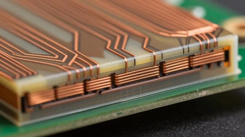
In the context of high-density flexible PCBs (FPCBs) for automotive keyless entry, the choice between traditional polyimide coverlays and photo-imageable coverlays (PIC) directly dictates the module's lifespan. Automotive environments demand thermal stability and vibration resistance; selecting the wrong dielectric can lead to stress-induced fatigue or moisture ingress, compromising sensitive RF performance.
| Coverlay Type | Mechanical Flexibility | Thermal Reliability | Density/Feature Size |
|---|---|---|---|
| Polyimide (PI) | Excellent | Superior | Moderate |
| Photo-Imageable (PIC) | Limited | Moderate | High |
Polyimide vs. Photo-Imageable: Trade-off Analysis
Standard polyimide films, typically bonded with acrylic adhesives, offer the best mechanical durability for dynamic flexing applications. However, their physical geometry—specifically the larger tolerances required for mechanical punching of access holes—makes them unsuitable for the ultra-fine pitch requirements of modern high-density interconnects. Conversely, photo-imageable coverlays allow for tight registration and smaller opening apertures, which are essential when designing dense circuitry for miniaturized keyless entry sensors.
- Why is adhesive thickness a DFM factor?
Excessive adhesive flow into high-density traces can create impedance discontinuities, while insufficient coverage may fail to protect against moisture-induced corrosion. - Does PIC affect flexibility?
Yes; PIC materials are inherently more brittle than polyimide. They should be restricted to static-flex regions rather than dynamic hinges in the key fob architecture. - How does this impact thermal cycling?
Coefficient of Thermal Expansion (CTE) mismatch between the coverlay and the base substrate can lead to delamination during automotive temperature cycling tests.
Trace Routing Strategies for Dynamic Flex Areas
Dynamic Routing Strategies for Flex Durability
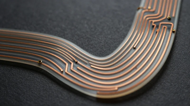
For keyless entry modules subjected to constant mechanical actuation, trace routing must transition from traditional rigid patterns to dynamic-optimized layouts. The primary goal is to minimize tensile stress and avoid the 'work hardening' of copper by distributing strain across wider radii and utilizing specific geometric routing techniques.
Optimizing Trace Geometry
When routing through active bending zones, avoid sharp 90-degree angles which create localized stress concentration points. Implementing curved or 'arc-based' routing ensures that mechanical forces are dispersed evenly across the length of the trace.
| Routing Technique | Mechanical Benefit | Best Application |
|---|---|---|
| Curved Arcs | Distributes strain | Critical signal paths |
| Staggered Traces | Prevents I-beam effect | High-density bundles |
| Neutral Axis Routing | Minimizes compression/tension | Extreme bend radii |
Essential DFM Best Practices for Fatigue Prevention
- How can I prevent the I-beam effect in multi-layer flex?
Stagger traces on adjacent layers so they are not directly stacked; this allows the circuit to remain more flexible and prevents stiffening caused by overlapping copper. - Is trace width critical in bend zones?
Yes, use thinner traces in bend areas if space permits, as wider traces have higher stiffness and are more prone to delamination and cracking under stress. - What is the importance of copper balancing?
Symmetrical copper distribution across layers prevents the flex circuit from twisting or 'curling' during thermal expansion and actuation, significantly increasing service life.
Designers should also consider the use of 'dummy' copper patterns or hatched ground planes to maintain structural symmetry while providing the necessary electromagnetic shielding for keyless entry communication protocols.
Managing Impedance Control in Tight Geometries
Managing Impedance Control in Tight Geometries
Maintaining consistent impedance in compact flexible circuits is fundamentally challenged by the reduction in trace width and the proximity to the reference plane. In keyless entry modules, where space is at a premium, engineers must account for the dielectric constant (Dk) fluctuations inherent in thin polyimide substrates and the dimensional instability that occurs during the lamination process. To achieve controlled impedance, designers must prioritize stack-up symmetry and employ tightly coupled differential pairs that minimize field leakage.
Critical Factors for Impedance Stability
| Parameter | Influence on Impedance | Design Mitigation |
|---|---|---|
| Dielectric Thickness | High | Specify tight-tolerance adhesive-less laminates |
| Trace Width Variation | High | Use laser-direct imaging (LDI) for fine features |
| Copper Surface Roughness | Moderate | Utilize low-profile (VLP) copper foils |
Frequently Asked Questions
- How does bending affect impedance?
Mechanical deformation shifts the distance between the signal trace and the reference plane, potentially altering the capacitance. Routing sensitive signals along the neutral axis of the flex circuit minimizes these variations. - Is a hatched ground plane necessary?
While solid planes offer better EMI shielding, they reduce flexibility. A properly designed hatched plane maintains impedance control while preserving the mechanical ductility required for high-cycle automotive applications. - What is the impact of coverlay on impedance?
The coverlay material acts as a secondary dielectric. Variations in adhesive thickness can shift impedance by several ohms, making thin, uniform adhesive-less coverlays superior for high-frequency signal integrity.
Optimizing Copper Weight for Mechanical Endurance
The Relationship Between Copper Thickness and Bend Radius
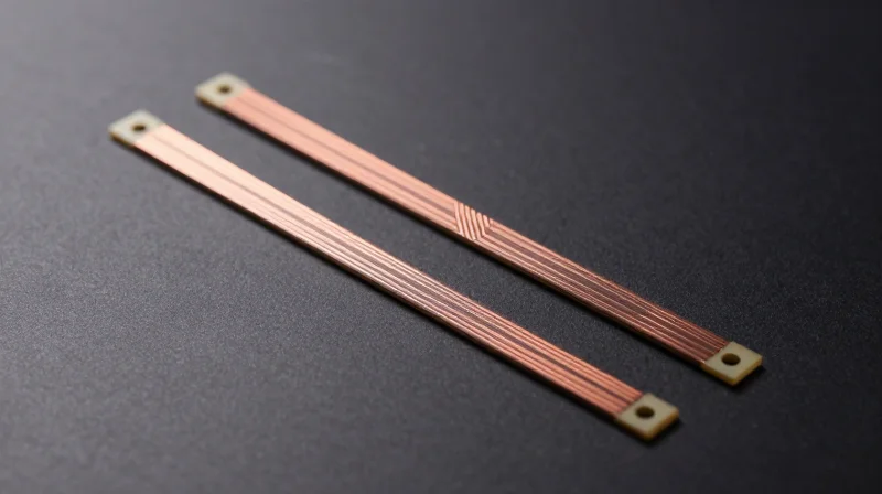
In high-density flexible designs, copper thickness acts as a mechanical anchor; thicker copper increases current carrying capacity but significantly raises the risk of trace fatigue and fracture during repeated bending. To maintain reliability in keyless entry modules, designers must specify the minimum copper weight capable of meeting thermal requirements without exceeding the strain limit of the conductive foil.
| Copper Weight (oz) | Approx. Thickness (mil) | Flexibility Profile | Typical Application |
|---|---|---|---|
| 0.33 (ED) | 0.47 | Excellent | Dynamic high-density flex |
| 0.5 (RA) | 0.7 | Good | Standard signal traces |
| 1.0 (RA) | 1.4 | Limited | Power distribution |
Best Practices for Mechanical Reliability
- Prioritize Rolled-Annealed (RA) Copper
Always specify RA copper over Electro-Deposited (ED) copper for dynamic applications; its grain structure is oriented to better accommodate mechanical strain without cracking. - Implement Neutral Axis Alignment
Position copper traces as close to the center of the polyimide stack-up as possible to minimize the tensile and compressive forces exerted during the bending radius. - Avoid Sharp Bends at Copper Edges
Ensure that wide copper planes are tapered or converted to hatched patterns when crossing flex regions to prevent localized stress concentrations.
Frequently Asked Questions
- Why is 1oz copper often discouraged in flex zones?
1oz copper is significantly more rigid than thinner foils, creating a larger moment arm that stresses the interface between the copper and the polyimide substrate, leading to premature fatigue. - How does hatch-patterned copper improve reliability?
Hatching reduces the overall cross-sectional area of the copper plane while maintaining current capacity, effectively increasing the 'effective' flexibility of the entire circuit layer.
Stiffener Design for Component Reliability
Strategic Stiffener Placement for Component Longevity
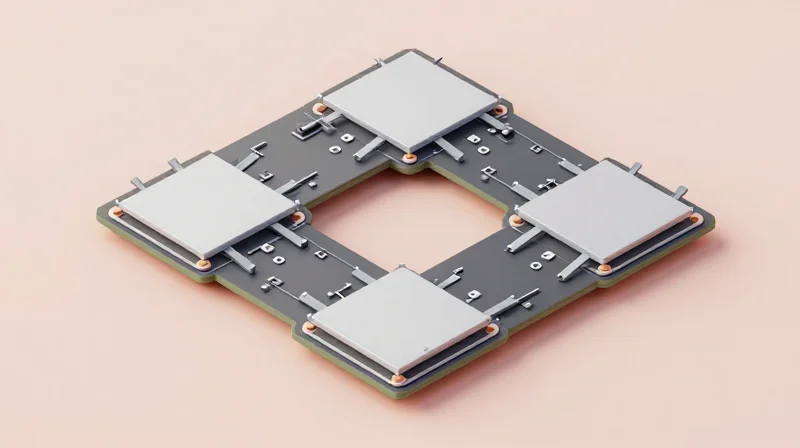
Stiffeners are mandatory in high-density flex designs, particularly where surface-mount components and connectors reside. By providing a rigid interface, stiffeners mitigate the risk of peeling, cracking, or solder joint fatigue caused by the inherent flexibility of the polyimide base. Proper application requires balancing material selection with geometry to prevent stress concentrations at the transition between the stiffened and flexible regions.
Material Selection and Application Standards
| Material Type | Common Use Case | Key Benefit |
|---|---|---|
| FR-4 | Connector interfaces | High rigidity and structural support |
| Polyimide | ZIF connector areas | Thermal stability and thickness matching |
| Stainless Steel | High-impact button arrays | Superior durability against repeated force |
Design Best Practices for Solder Joint Protection
- Transition Zone Management
Always ensure the stiffener edge is offset from the pad edge by at least 0.5mm to prevent stress fractures in the copper at the rigid-flex boundary. - Adhesive Integrity
Use pressure-sensitive or thermally cured acrylic adhesives to ensure uniform bonding, as inconsistent adhesive thickness leads to uneven stress distribution during thermal cycling. - Connector Anchoring
For connectors experiencing insertion force, extend the stiffener underneath the entire footprint and include secondary anchor points to isolate the solder joints from mechanical strain.
Adhering to these DFM rules is critical for the long-term reliability of keyless entry modules, which are subject to high-frequency mechanical inputs. Designers must treat the stiffener not merely as a structural support but as a thermal and mechanical decoupler that protects the delicate interconnects of the high-density circuit.
Via-in-Pad and Plating Best Practices
Via-in-Pad Implementation for Flex
In high-density flexible designs, utilizing via-in-pad (VIP) technology is essential for space constraints, but it necessitates specific DFM measures to prevent component solder starvation and cracking. Always ensure that vias located within pads are fully plugged and capped with conductive or non-conductive epoxy to maintain a flat surface and prevent solder wicking into the barrel.
Plating Best Practices
Uniform copper distribution is critical in flexible circuits to ensure both electrical reliability and mechanical longevity. Variations in plating thickness can create stress risers, which, when combined with the repeated bending cycles characteristic of keyless entry modules, lead to early fracture.
| Process Parameter | Best Practice | Reasoning |
|---|---|---|
| Copper Plating | Pulse Plating | Achieves uniform thickness in high-aspect-ratio holes. |
| Via Finish | Epoxy Fill + Capped | Prevents solder wicking and provides planar surface. |
| Panel Layout | Copper Balancing | Reduces stress during chemical etching and plating. |
Frequently Asked Questions
- Why is conductive epoxy preferred for via filling?
Conductive epoxy is generally preferred in power-delivery paths where maintaining electrical continuity and thermal conductivity is critical across the via structure. - Does plating thickness impact flexibility?
Yes. Over-plating increases the stiffness of the flexible circuit, which can lead to fatigue cracking at the transition zones near stiffeners. - How do you avoid dimpling in via-in-pad?
Use a specialized planarization process after the epoxy fill to ensure the cap plating is flush with the surrounding pad surface.
Testing Protocols for Flex Circuit Validation
Testing Protocols for Flex Circuit Validation
Validating high-density flexible PCBs for keyless entry modules requires a dual-track approach: verifying the electrical signal integrity under static conditions and testing the physical robustness of the circuit during dynamic bending cycles. Since these modules are subjected to constant vibration and repeated mechanical stress, validation protocols must exceed standard IPC-6013 Class 3 requirements to ensure long-term field reliability.
Dynamic and Mechanical Benchmarks
| Test Method | Target Metric | Pass/Fail Criteria |
|---|---|---|
| MIT Flex Life Test | 10,000+ cycles | No trace cracking or delamination |
| Rolling Flex Test | Min bend radius (10x thickness) | Resistance shift < 5% |
| Solder Joint Stress | Thermal shock -40C to 125C | Zero intermittent open circuits |
Electrical Integrity and Reliability FAQ
- How is intermittent signal loss detected in flex circuits?
We utilize high-speed event detectors (HSED) that monitor for resistance spikes exceeding 10 ohms during the entire duration of the mechanical flex testing process. - Why is TDR (Time Domain Reflectometry) testing mandatory for keyless entry modules?
TDR testing ensures that high-density impedance lines remain within spec even after the substrate has been subjected to forming or bending during the assembly process. - What is the role of High-Pot testing in this validation process?
High-potential dielectric withstand testing is critical to verify that the polyimide coverlay and adhesive systems haven't developed micro-voids or thinning that could lead to short circuits in humid, automotive environments.
Mastering these DFM rules is essential for scaling sophisticated keyless entry technology. By prioritizing material selection, stress-managed routing, and robust component support, you ensure your product remains reliable under the most demanding conditions. Ready to refine your design process? Contact our engineering team today for a comprehensive DFM audit of your next project.
