
In the world of vertical transportation, zero failure is the only acceptable standard. For elevator control systems, PCB design isn't just about functionality; it's about life-safety and relentless continuous operation. If your design-for-manufacturing (DFM) process misses the mark, you risk costly field failures and compromised safety. This guide explores the advanced DFM rules required to build boards that stand the test of time.
The Criticality of DFM in Elevator Control Systems
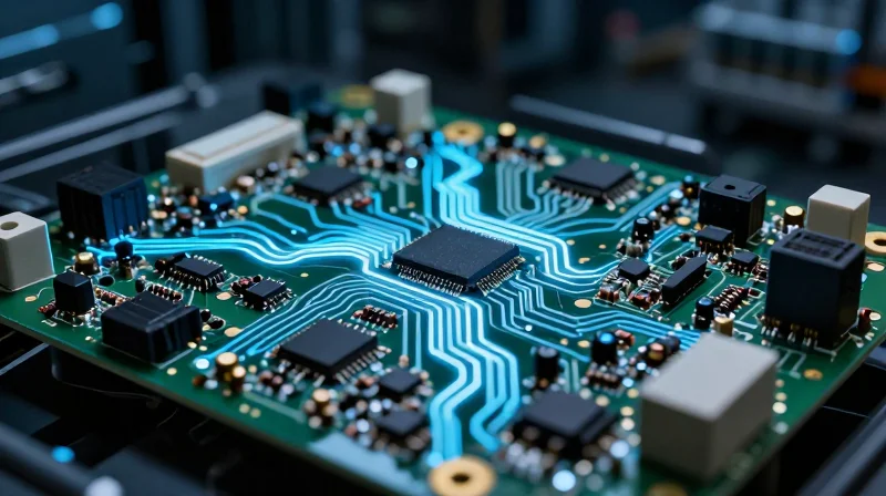
In the high-stakes environment of vertical transportation, elevator control PCBs are the mission-critical brains governing safety, movement, and diagnostics. Implementing advanced DFM rules is not merely an optimization exercise; it is an essential safeguard against the mechanical and environmental stresses intrinsic to elevator shafts. Failure to prioritize DFM during the PCB design phase frequently leads to premature hardware degradation, intermittent sensor faults, and the high cost of field-service interventions.
The Risk Profile of Non-Compliant Designs
When PCB designs ignore standard DFM practices, they introduce micro-vulnerabilities that propagate through the manufacturing line and into the field. These risks are amplified by the harsh, non-climate-controlled environment of many elevator shafts.
| DFM Oversight | Manufacturing Consequence | Field Impact |
|---|---|---|
| Inadequate Thermal Vias | Excessive heat buildup | Component failure & system shutdown |
| Tight Trace/Pad Tolerance | Soldering bridging risks | Intermittent shorts & ghost errors |
| Poor Component Placement | Assembly yield drops | Vibration fatigue & connector failure |
DFM Implementation: Frequently Asked Questions
- Why is trace geometry critical in elevator control?
Elevator systems often involve inductive loads and high-speed switching; improper trace width or spacing leads to electromagnetic interference that can cause erroneous floor positioning or safety brake engagement. - Does DFM impact long-term maintenance costs?
Yes. Optimized DFM ensures high-quality solder joints and robust board integrity, significantly reducing the probability of intermittent hardware failures that require expensive, onsite technician visits to non-standard shaft environments. - What is the biggest mistake in elevator PCB DFM?
Underestimating thermal management. Elevator controllers operate continuously; designs that lack proper copper pours or heat-sinking strategies will inevitably face shortened component lifespans due to thermal cycling fatigue.
Optimizing Thermal Management for Constant Load
Heat Dissipation Strategies for High-Reliability Systems
Constant operation in elevator control cabinets demands rigorous thermal mitigation to prevent localized hot spots that trigger premature component aging. Designing for thermal longevity requires moving beyond passive heat sinks toward an integrated PCB-level architecture that utilizes the board substrate itself as a thermal conduit.
Strategic Copper Pours and Thermal Plane Integration
Designers should leverage internal layers as dedicated ground or power planes to serve as thermal heat spreaders. By increasing the copper weight (e.g., 2oz instead of 1oz) in these layers, the board can effectively conduct heat away from critical MOSFETs and MCU packages to the board periphery, where chassis-coupling or airflow can extract the energy.
| Strategy | Thermal Impact | Manufacturing Complexity |
|---|---|---|
| 2oz Copper Planes | High dissipation/Low impedance | Medium (Requires longer etch time) |
| Thermal Via Arrays | Vertical heat transfer | Low |
| Component Staggering | Reduced localized flux | Low |
Optimizing Thermal Via Placement
Thermal vias must be placed directly under the thermal pads of high-power components. To prevent 'solder wicking' (which can lead to dry joints), designers should utilize capped or epoxy-filled vias where possible. The grid density for these vias should follow a pitch of approximately 1.0mm to 1.27mm to ensure maximum copper-to-air contact without violating mechanical integrity.
- How does component density affect thermal load?
High component density clusters create 'thermal zones' where heat cannot escape, requiring significantly more copper pours and forced convection to maintain safe operating temperatures. - Why is board thickness relevant to thermal management?
A thicker board increases the thermal mass, acting as a larger heat sink, though it simultaneously limits vertical heat transfer between layers unless high-density via stitching is employed.
Ensuring Signal Integrity in Harsh Environments
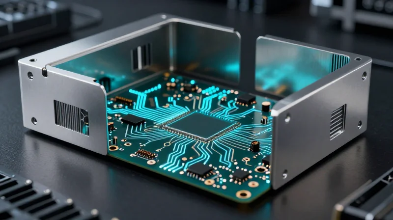
Elevator shafts are electrically noisy environments, dominated by high-voltage motor currents, relay switching, and fluctuating magnetic fields. To maintain stable communication and signal fidelity, PCB designs must adhere to strict EMI mitigation protocols. Implementing controlled impedance, strategic layer stack-up, and robust grounding architectures is essential to prevent data corruption and unexpected system failures.
Mitigating Crosstalk and EMI
Crosstalk in high-speed digital lines is primarily managed through geometry control. Maintaining a distance between signal traces at least three times the dielectric height (3W rule) is a fundamental DFM requirement. Furthermore, utilizing differential pairs with precise length matching ensures that common-mode noise is rejected by the differential receiver, effectively neutralizing the interference generated by high-power elevator motors.
| Technique | Primary Benefit | Implementation Rule |
|---|---|---|
| Differential Routing | Noise Immunity | Ensure equal length within 5 mils |
| Ground Plane Stitching | EMI Shielding | Via pitch < 1/10th of signal wavelength |
| Guard Traces | Crosstalk Reduction | Ground vias at both ends of the guard |
Best Practices for Stack-up and Grounding
The stack-up architecture serves as the foundation for EMI control. A solid reference plane located directly beneath high-speed signals is non-negotiable, as it provides a low-impedance return path that minimizes loop area. In multi-layer boards, interleaving signal layers between ground planes (stripline configuration) provides significant shielding against external electromagnetic fields common in industrial elevator shafts.
- How do I handle split ground planes?
Avoid splitting ground planes under high-speed signals. If different ground domains are necessary, bridge them only at the point of signal transition to prevent massive return path loops. - What is the role of decoupling capacitors?
Place low-ESR decoupling capacitors as close to IC power pins as possible to suppress local power plane noise, which would otherwise radiate as EMI. - Is via shielding effective for signal edges?
Yes, surrounding sensitive signals with a perimeter of ground vias (stitching) effectively creates a Faraday cage within the PCB substrate.
Robust Material Selection and PCB Stack-up
Material Selection for High-Stress Environments
Elevator control units operate in environments characterized by extreme temperature cycling and mechanical vibration. Standard FR-4 laminates often succumb to delamination or barrel cracking under these conditions. Engineers should specify high-Tg (Glass Transition Temperature) materials, typically exceeding 170°C, to ensure stable dielectric constants and reliable thermal expansion coefficients (CTE) across the operational lifespan.
| Material Property | Standard FR-4 | High-Tg/High-Reliability |
|---|---|---|
| Tg (Glass Transition) | 130-140°C | 170-180°C+ |
| Thermal Expansion (Z-axis) | High | Low (Controlled) |
| Vibration Resilience | Moderate | Excellent |
| Application Suitability | General Office/IT | Industrial/Elevator |
Optimizing Stack-up for Structural Integrity
A symmetrical layer stack-up is mandatory to prevent board warping during reflow soldering and throughout the service life of the PCB. Placing heavy copper planes in the internal layers not only aids in power distribution but also provides the structural rigidity necessary to counteract mechanical vibrations typical of high-speed elevator shafts.
Frequently Asked Questions on Stack-up and Finish
- Why is surface finish critical for elevator controls?
ENIG (Electroless Nickel Immersion Gold) is preferred over HASL for high-density boards, providing superior flatness and protection against oxidation, which is vital for long-term connector reliability. - How does stack-up symmetry affect reliability?
Asymmetric layouts lead to differential thermal expansion between layers, causing the board to bow or twist, which places undue stress on solder joints and vias. - Is thicker copper recommended for all layers?
No; while thicker copper (e.g., 2oz) is excellent for power integrity and heat dissipation, it must be balanced with thinner signal layers to maintain precise trace impedance and avoid manufacturing etch-factor issues.
Assembly Design Rules: Beyond Standard SMT
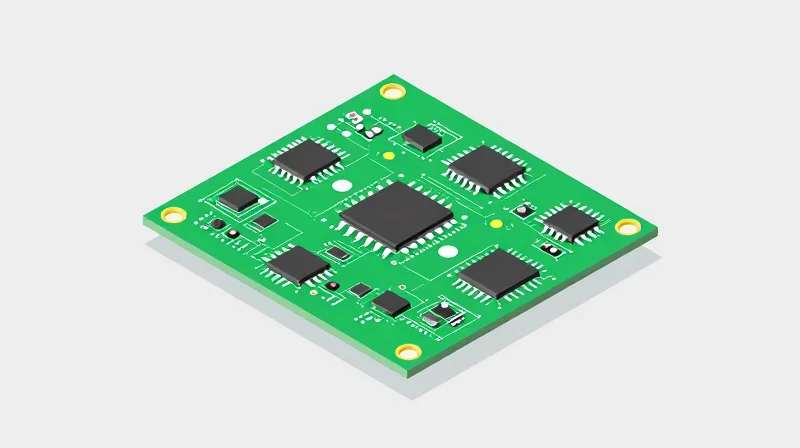
Advanced Stencil Engineering for High-Reliability Assemblies
Standard stencil design often fails to account for the mechanical stresses present in elevator shafts. To ensure long-term reliability, we employ multi-level stencils and aperture modifications that maximize solder volume for large-pad components, such as power MOSFETs and microcontrollers, while reducing voiding in thermal relief areas.
| Feature | Standard SMT Practice | Advanced Elevator DFM |
|---|---|---|
| Aperture Scaling | 1:1 ratio | 85-90% reduction on fine pitch |
| Solder Volume | Uniform depth | Increased for high-mass components |
| Aperture Shape | Rounded rectangles | Home-plate or U-shaped for stress relief |
Footprint Optimization and Mechanical Robustness
Component footpaths must be designed with an emphasis on vibration damping and shear resistance. By implementing extended toe fillets and ensuring thermal pads are anchored via non-tented vias, we significantly improve the mechanical bond between the PCB and the control hardware.
Assembly Design FAQ
- Why avoid tented vias for thermal pads?
Tenting traps air, causing outgassing during reflow, which results in massive solder voiding that compromises heat transfer and structural integrity. - How do you manage vibration-induced fatigue?
We specify secondary adhesive staking for large capacitors and utilize longer, more ductile solder fillets to accommodate cyclical mechanical stress. - Is localized underfill necessary?
For high-I/O BGA components located near high-vibration connectors, underfill is strongly recommended to redistribute mechanical load away from fragile solder balls.
Managing Mechanical Stress and Board Flex
Engineering for Structural Integrity
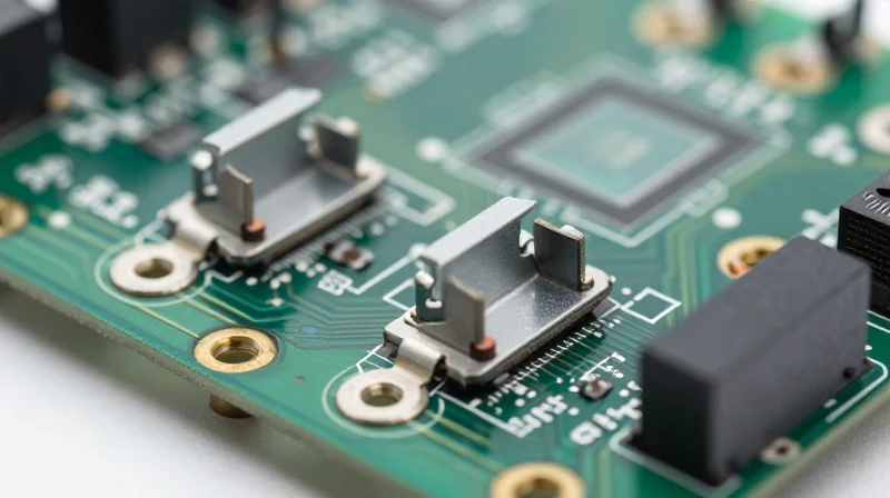
Elevator control systems face continuous mechanical vibrations and structural shifts throughout their operational lifespan. To prevent solder joint fatigue and micro-cracking, board design must prioritize physical rigidity and intelligent stress distribution through precise mounting point placement.
Managing Board Flex through Component Placement
Large or heavy components act as potential stress concentrators during board bending. Keep high-mass components away from board edges and minimize the proximity of delicate BGA packages to mounting holes, which are frequent initiation points for PCB delamination or fractures.
| Design Element | Risk Factor | Mitigation Strategy |
|---|---|---|
| Mounting Holes | Stress Concentration | Keep components >5mm away from hole edges |
| Panel Breakouts | Edge Cracking | Route V-scores far from sensitive circuitry |
| Tall Capacitors | Leverage Force | Use underfill or secondary mechanical clamping |
Structural Reinforcement Best Practices
- How do board stiffeners affect assembly?
Stiffeners significantly increase the localized Young's modulus of the board, preventing flex during connector insertion; ensure these are grounded if they are conductive to avoid EMI issues. - Why is mounting point symmetry important?
Asymmetric mounting forces can cause latent warping during thermal cycling; distributing mounting holes evenly across the board profile maintains a neutral mechanical balance. - What role does solder mask play in structural health?
Excessive solder mask between fine-pitch pads can act as a brittle point; prioritize smooth transitions and avoid thick 'dams' near stress-prone board segments.
Ultimately, the longevity of elevator control PCBs in rugged environments depends on the combination of material thickness—typically 2.4mm to 3.2mm for high-vibration scenarios—and the strategic deployment of structural supports to ensure the assembly remains planar under load.
Testing Protocols: DFM for In-Circuit Test (ICT)
Integrating ICT Requirements into PCB Layout
For critical elevator control systems, In-Circuit Test (ICT) is non-negotiable for validating solder joints and component functionality at a granular level. Designers must prioritize accessibility for bed-of-nails fixtures by implementing test pads on all primary nets, ensuring that critical safety signals can be interrogated post-assembly without causing mechanical damage to the high-density components characteristic of modern elevator controllers.
Standardizing Test Point Geometry and Placement
| Feature | Recommended DFM Specification | Reasoning |
|---|---|---|
| Test Pad Diameter | 0.8mm to 1.0mm | Ensures reliable probe contact and reduces sliding. |
| Center-to-Center Spacing | 2.54mm (0.100") | Standardizes probe sizing for lower fixture costs. |
| Edge Clearance | 3.0mm minimum | Prevents board warping during vacuum fixture engagement. |
| Solder Mask | Tented or Clear | Prevents probe contamination and ensuring conductive contact. |
Frequently Asked Questions: ICT Best Practices
- Can test points be placed on the bottom side only?
While single-sided access is preferred to reduce fixture costs, complex elevator control logic often necessitates dual-sided access; ensure alignment holes are included for registration. - How does ICT affect board reliability?
Improper probe pressure can cause pad lifting or board deflection; always specify test points on stable support areas and avoid placing them near delicate fine-pitch SMT connectors. - What is the impact of conformal coating on ICT?
If boards are coated post-test, ensure testing is completed before the application of moisture-resistant resins, as coating residues will insulate test pads and cause false failures.
By adhering to these DFM protocols, manufacturers ensure that the elevator control board not only meets performance specs but is also fully inspectable throughout its lifecycle. Precision in probe placement mitigates mechanical stress and facilitates rapid diagnostics during the critical high-volume manufacturing phase.
Documentation and Collaboration with Manufacturers
The Critical Role of Comprehensive Documentation
Precision manufacturing starts with a complete data package that eliminates ambiguity. For complex elevator control systems, specifications must go beyond basic Gerber files. A robust documentation set includes IPC-Class 3 compliant drawings, detailed layer stack-up definitions with impedance control requirements, and explicit surface finish specifications. Providing a clear Bill of Materials (BOM) with validated manufacturer part numbers (MPNs) ensures that component sourcing does not compromise the board's reliability under the high-vibration environment of an elevator hoistway.
Essential Elements of a Manufacturing Data Package
| Document Type | Purpose | Key Detail Required |
|---|---|---|
| Fabrication Drawing | Outlines critical board dimensions | Controlled impedance and stack-up |
| Assembly Drawing | Defines component orientation | Clear polarity and keep-out zones |
| BOM | Lists all materials | Validated MPN and lifecycle status |
| Readme/Special Instructions | Communicates custom constraints | Solder mask and finish thickness |
Fostering Collaboration for Design Integrity
Direct engagement with the PCBA partner’s engineering team during the design phase—known as Design for Manufacturing (DFM) consultation—is a powerful strategy to prevent assembly defects. Proactive communication regarding specialized materials, such as thermal interface compounds or specific coating requirements for elevator control logic, allows manufacturers to optimize their processes before production begins.
- Why should DFM reviews occur before final board sign-off?
Early engagement identifies footprint errors or panelization inefficiencies that would otherwise trigger costly hold-ups or rework on the production line. - How does open communication mitigate assembly risks?
Sharing your intended operating environment helps the manufacturer select appropriate solder alloys and conformal coating application methods that match your thermal and vibration requirements. - What is the best way to handle engineering change orders (ECOs)?
Implement a formal revision control system within your documentation package to ensure the manufacturer is always working from the most recent, approved design iteration.
High-reliability elevator control is a marriage of meticulous design and precise manufacturing. By implementing these advanced DFM rules, you protect your system from environmental degradation and extend the service life of your electronics. Ready to optimize your hardware for the field? Contact our engineering team today to review your current PCB design and ensure peak reliability for your next project.
