
Designing high-current power distribution units (PDUs) pushes standard PCB manufacturing to its physical limits. When your board handles hundreds of amps, standard signal-integrity rules no longer apply—thermal management and mechanical stability become the primary determinants of product lifespan. This guide breaks down the essential DFM protocols required to ensure your high-power designs survive the manufacturing floor and perform reliably in the field.
Calculating Precise Copper Weights and Trace Widths
Beyond IPC-2221: Embracing IPC-2152
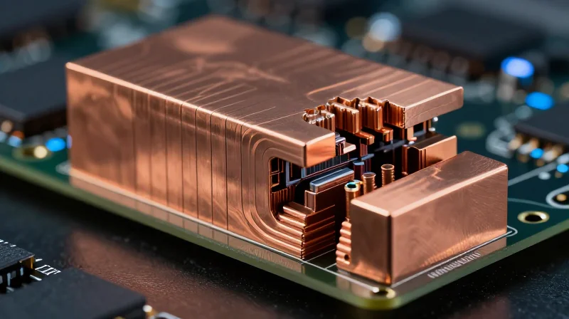
While the legacy IPC-2221 standard has served the industry for decades, it is frequently insufficient for modern high-current Power Distribution Unit (PDU) designs. IPC-2221 often underestimates the required trace widths for specific temperature rises because it relies on simplified geometric curves that ignore complex thermal environments. Designers must transition to IPC-2152, which utilizes advanced physics-based modeling to account for board thickness, copper weight, dielectric properties, and the surrounding thermal assembly, ensuring a more accurate prediction of the conductor temperature.
Calculating for High-Current Density
When calculating trace dimensions for high-current applications, one must account for the cross-sectional area of the copper. A common pitfall is ignoring the reduction of copper thickness due to electroplating variations or etching processes. For high-current PDUs, designers should specify the final finished copper weight—typically 2oz, 3oz, or higher—and apply derating factors for internal layers versus external layers.
| Design Factor | Impact on Thermal Performance | Mitigation Strategy |
|---|---|---|
| Internal Layers | Higher thermal resistance | Increase trace width by 30-50% vs external |
| Thermal Vias | Lowers local junction temp | Implement thermal via stitching arrays |
| Copper Weight | Reduces electrical resistance | Specify heavy copper (3oz+) for power planes |
Frequently Asked Questions
- Why is IPC-2221 considered outdated for high-current PDUs?
IPC-2221 lacks the multi-variable depth of IPC-2152, failing to account for board material thermal conductivity and the cooling effect of the assembly, which can lead to premature trace failure. - How do copper busbars compare to PCB traces?
Copper busbars provide significantly larger cross-sectional areas and superior heat sinking. Integrating these with high-current PCBs allows for localized high-amperage routing that would be physically impossible on a standard laminate. - What is the primary risk of undersized traces in a PDU?
Undersized traces lead to excessive ohmic heating, which causes thermal degradation of the PCB substrate (delamination, measling) and increases the risk of catastrophic failure under peak load conditions.
Advanced Thermal Relief Design Patterns
The Thermal Relief Dilemma: Assembly vs. Performance
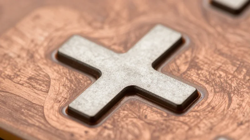
In high-current Power Distribution Units (PDUs), traditional thermal relief patterns often act as bottleneck resistors. While a standard four-spoke relief pattern simplifies manual rework and prevents cold solder joints by limiting heat dissipation into the ground plane during reflow, it significantly restricts current density. Advanced designs must transition toward localized thermal management that maintains solderability without compromising electrical integrity.
Strategic Relief Geometry Comparison
| Relief Pattern Type | Solderability Benefit | High-Current Capacity | Best Use Case |
|---|---|---|---|
| Four-Spoke Standard | Excellent | Low | Signal/Low-Power Pins |
| Heavy-Duty Solid Connection | Poor (requires pre-heat) | Very High | Power/Ground Terminals |
| Thickened Multi-Spoke | Moderate | High | High-Current Connectors |
Optimized Pattern Implementation
To achieve a balance, designers should implement 'Thickened Multi-Spoke' patterns. By increasing the width of the spokes and reducing the air-gap clearance, you maintain a degree of thermal isolation for the solder joint while maximizing the cross-sectional area available for current flow. In extreme current applications, moving to a solid thermal connection is preferred if the assembly process utilizes vapor phase soldering or specialized infrared pre-heating to negate the potential for cold joints.
Frequently Asked Questions
- When is it safe to use solid copper connections for power pads?
Solid connections are safe when the board assembly process includes high-wattage pre-heating to prevent the PCB plane from acting as a massive heat sink during soldering. - How do I calculate the current impact of thermal relief spokes?
Treat each spoke as an individual trace. Use IPC-2152 to determine the allowable current based on the width and length of each spoke, then sum the total capacity for all spokes connected to the pad. - Can solder masks be used to improve thermal performance?
While solder masks do not improve conductivity, using 'solder mask defined' pads for power components can help ensure precise pad geometry, preventing unwanted solder wicking into thermal relief gaps.
Managing Layer Delamination in Heavy Copper Boards
Mitigating CTE Mismatches in High-Copper Laminates
Layer delamination in heavy copper boards (typically 3oz or higher) is primarily driven by the CTE mismatch between the bulk copper conductors and the surrounding glass-reinforced epoxy resin. When high-current surges induce rapid thermal cycling, the copper layers expand at a different rate than the dielectric material, creating intense shear stress at the resin-to-copper interface. To prevent mechanical failure, engineers must prioritize high-Tg (glass transition temperature) and low-CTE substrates that provide superior dimensional stability.
| Material Property | Standard FR-4 | High-Performance/Heavy Copper Laminate |
|---|---|---|
| Glass Transition Temperature (Tg) | 130-140°C | 170-185°C+ |
| CTE (Z-axis, below Tg) | 50-70 ppm/°C | <35 ppm/°C |
| Copper Peel Strength | Moderate | High (Treated Foils) |
Best Practices for Substrate Selection
- Why is a high Tg critical for heavy copper?
Materials with a high Tg maintain their structural integrity at higher temperatures, preventing the resin from becoming soft and losing its adhesion to heavy copper features during peak thermal excursions. - How does filler content influence reliability?
Ceramic-filled dielectrics provide a significantly lower CTE, effectively anchoring the copper features and preventing the 'pull-away' effect common in standard resin systems. - Should I use treated copper foils?
Yes; specifically using low-profile, double-treated copper foils enhances the mechanical interlocking between the copper and the dielectric, which is essential for resisting the shear forces generated by heavy current paths.
Beyond substrate selection, DFM rules should mandate balanced copper distribution across the stackup. Large, unpopulated planes of heavy copper should be balanced with thermal relief patterns or 'copper thieving' on opposing layers to prevent board warpage during lamination and subsequent assembly stages, ensuring long-term structural reliability.
Copper Busbar Integration and Mechanical Anchoring
Mechanical Anchoring and Stress Mitigation
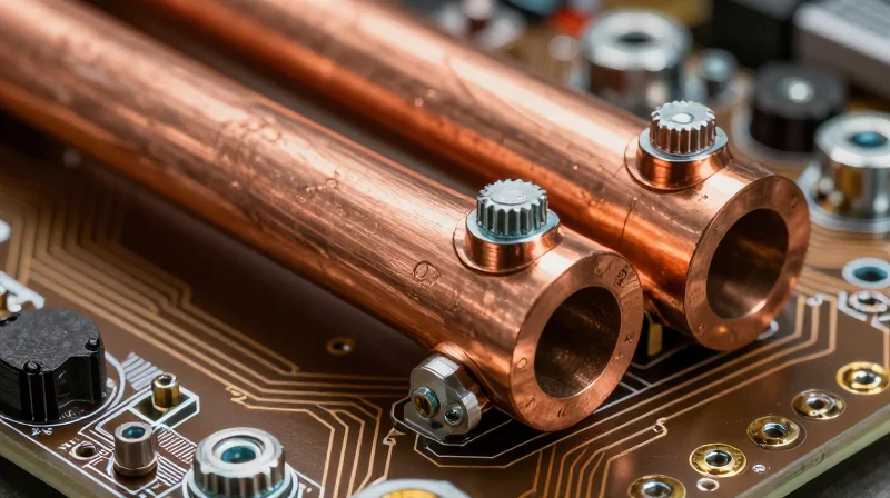
Mechanical anchoring is the primary defense against long-term fatigue in PDU assemblies. Because copper busbars possess a significantly different coefficient of thermal expansion (CTE) than FR-4 or high-Tg PCB substrates, direct-solder connections alone are insufficient for heavy-current applications. Designers must implement mechanical fasteners, such as press-fit studs or bolted standoffs, to isolate the electrical joint from mechanical vibration and thermal cycling-induced strain. Ensuring a coplanar mounting surface and utilizing slotted holes for bolt clearance can compensate for thermal expansion, preventing the busbar from acting as a lever that exerts torque on the PCB's via barrels and solder pads.
Optimizing Contact Resistance
Achieving ultra-low contact resistance requires a multi-faceted approach to surface preparation and compression. For bolted connections, the contact patch must be cleaned and treated to prevent oxidation, while the contact pressure must be calibrated to exceed the yield strength of the copper surface without deforming the PCB substrate.
| Interface Method | Reliability Profile | Best Use Case |
|---|---|---|
| Surface Mount Soldering | Low | Low-current, automated assembly |
| Press-fit Studs | High | High-vibration, automotive/industrial |
| Through-hole Bolted | Very High | High-current busbar power distribution |
Frequently Asked Questions
- How do I prevent solder joint cracking under busbar weight?
Utilize dedicated mechanical anchoring, such as mounting screws or brackets, to carry the physical weight of the busbar, ensuring the solder joint only manages the electrical connection rather than structural support. - What is the recommended surface finish for busbar interface pads?
ENIG or ENEPIG are preferred for their superior planarity and oxidation resistance compared to HASL, which provides a more consistent contact surface for high-current mating. - Does thermal expansion impact bolted joints?
Yes, thermal cycling can loosen bolts; use Belleville spring washers to maintain consistent clamping force across a wide range of operating temperatures.
Optimizing Via Arrays for Current Carrying and Heat Dissipation
Via-in-Pad and Stitching Strategies for Thermal Management
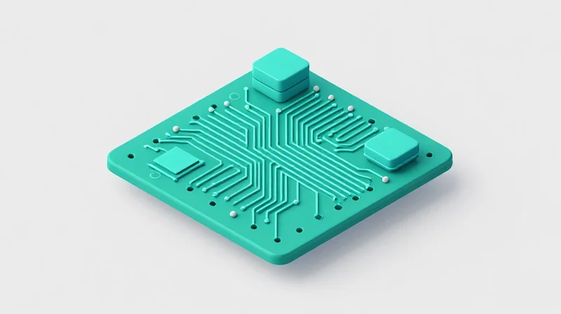
In high-current power distribution units, copper weight alone is often insufficient to dissipate heat generated by MOSFETs and power ICs. By implementing dense via-in-pad arrays, designers create a direct, low-thermal-resistance path from the component land to internal ground or power planes. This configuration minimizes the thermal interface resistance and allows the entire PCB copper stack to act as a heat spreader.
| Via Feature | High-Current Design Requirement | Impact on Performance |
|---|---|---|
| Via Diameter | 0.2mm to 0.3mm | Balances plating capability with copper volume. |
| Via Pitch | 0.5mm to 0.8mm | Prevents thermal saturation and maintains board rigidity. |
| Plating Thickness | 25µm minimum | Reduces resistance and increases current carrying capacity. |
Mechanical and Thermal Integration FAQ
- Why is copper-filled via-in-pad preferred for high-current applications?
Copper-filled vias provide superior thermal conductivity compared to epoxy-filled alternatives and ensure a solid landing surface for component pins, preventing solder wicking and voids. - How does via stitching affect PCB delamination risks?
Excessive via density can compromise board structural integrity. Designers must balance the number of vias with the PCB substrate's CTE to prevent micro-cracking during thermal cycling. - Is there a limit to how much current a via array can carry?
Current capacity is limited by the total surface area of the barrel copper. Always use IPC-2152 guidelines to calculate the temperature rise for a specific current load based on the via count and plating thickness.
Implementation Best Practices
For optimal results, ensure all stitching vias are tied to large thermal relief patterns on internal layers. Avoid grouping vias too tightly in a single corner of the component pad; instead, distribute them evenly across the thermal footprint to avoid local hot spots that lead to board warping. When integrating busbars, ensure that the vias under the mounting points are reinforced with additional annular rings to handle mechanical stress alongside electrical current.
Surface Finish Considerations for Power Reliability
Surface Finish Performance for High-Power Applications
In high-current Power Distribution Units (PDUs), the surface finish serves as the critical interface between the PCB copper traces, busbar mounting points, and active power components. Under high-temperature operation, intermetallic compounds (IMC) can grow rapidly, leading to brittle solder joints and increased contact resistance. Choosing a finish that maintains structural integrity and oxidation resistance is mandatory for long-lifecycle reliability.
| Surface Finish | Oxidation Resistance | High-Temp Stability | Ideal Application |
|---|---|---|---|
| HASL (Lead-Free) | Moderate | Moderate | General power boards |
| ENIG | Excellent | High | Fine-pitch/High-reliability |
| Immersion Silver | Moderate | Low | Busbar contact points |
Comparative Reliability Factors
- Is HASL suitable for high-current busbar interfaces?
HASL provides thick solder coverage which is beneficial for mechanical strength, but its uneven surface can lead to non-coplanar busbar seating, creating localized hot spots due to inconsistent contact pressure. - How does ENIG manage long-term thermal aging?
ENIG offers superior oxidation resistance, but designers must strictly control nickel thickness to prevent the 'black pad' phenomenon, which can compromise the integrity of high-current power joints. - Why is Immersion Silver risky for high-heat environments?
Immersion Silver provides a highly conductive surface, but it is prone to tarnish and creep corrosion in humid, high-temperature environments, potentially leading to dendritic growth between high-voltage traces.
For PDUs requiring integration with copper busbars, ENIG (Electroless Nickel Immersion Gold) is the professional standard for mating surfaces due to its flat topography and consistent nickel barrier. However, if the design involves massive solder-reflow requirements for through-hole power components, High-Temperature Organic Solderability Preservative (OSP) or thick Lead-Free HASL is often preferred to avoid the inherent fragility of the ENIG nickel interface under thermal cycling stress.
Manufacturing Assembly Protocols and Inspection Criteria
Creepage and Clearance Optimization
Maintaining strictly controlled isolation distances is non-negotiable for high-current systems. Designers must calculate minimum spacing based on peak operating voltage and pollution degree environments, often requiring PCB slots or milled cavities when surface clearance is insufficient to meet IEC 60664-1 standards.
| Requirement | DFM Protocol | Verification Method |
|---|---|---|
| Creepage | Increase surface path via slots | Automated Optical Inspection (AOI) |
| Clearance | Maintain air gap per voltage | High-potential (Hi-Pot) test |
| Solder Mask | Eliminate bridges on HV nodes | Cross-section analysis |
Solder Mask and Assembly Reliability
High-current PDUs require precise application of solder mask to prevent dielectric breakdown and flux entrapment. Proper mask dams are essential between high-voltage busbar mounting points, as moisture accumulation in narrow gaps can lead to conductive anodic filament (CAF) formation and catastrophic short circuits.
Inspection Criteria FAQ
- How is solder mask clearance verified for busbars?
Solder mask should be pulled back at least 0.1mm from mounting holes to prevent interference with physical connections while maintaining enough dielectric coverage to prevent arc tracking. - What is the role of Hi-Pot testing in assembly?
Hi-Pot testing verifies that the assembled product maintains isolation under surge conditions, identifying hidden defects like solder whiskers or insufficient creepage caused by assembly variances. - Why is flux residue management critical?
In high-current applications, residual acidic flux can act as a catalyst for oxidation and ion migration over time, potentially bridging high-potential circuits during humid environmental exposure.
Achieving long-term reliability in high-current electronics requires a shift in focus from mere signal flow to robust mechanical and thermal engineering. By strictly adhering to these DFM protocols, you mitigate the risk of catastrophic field failures and costly manufacturing delays. Ready to optimize your next high-power design? Contact our engineering team today for a comprehensive DFM audit of your PCB files.
