
The demand for immersive AR/VR experiences is pushing PCB manufacturing to its absolute limits. As form factors shrink and frame rates climb, the margin for error in signal integrity vanishes. In this guide, we dive into the veteran-level DFM strategies required to navigate the complexities of High-Density Interconnect (HDI) boards, ensuring your high-speed designs move from prototype to production without performance degradation.
The High-Frequency Challenge in AR/VR Wearables

The High-Frequency Challenge in AR/VR Wearables
Designing for high-frame-rate AR/VR headsets demands unprecedented data throughput, pushing signal speeds into the multi-gigabit range. This high-frequency environment transforms standard interconnects into complex transmission lines where parasitic capacitance and inductance threaten signal integrity. In compact wearable form factors, the requirement for high-density interconnect (HDI) substrates exacerbates these issues, as trace proximity increases the likelihood of crosstalk and electromagnetic interference (EMI), forcing designers to adopt rigorous DFM practices to maintain image fidelity and system reliability.
Key Design Constraints
| Constraint | Impact on Signal Integrity | DFM Mitigation Strategy |
|---|---|---|
| Trace Density | Increased crosstalk and signal coupling | Implement strictly controlled differential pair spacing |
| Via Stubs | Resonant reflections causing signal degradation | Utilize back-drilling or blind/buried via technology |
| Thermal Density | Impedance drift due to temperature swings | High-Tg materials and optimized copper pouring for dissipation |
Common Implementation Questions
- How does extreme miniaturization impact EMI?
As traces are packed tighter to support high-density routing, the magnetic fields overlap more easily. This requires advanced shielding techniques and precise impedance control across every layer transition. - Why are thermal bottlenecks critical for frame rates?
High frame rates demand high processing power, which generates localized heat. Because dielectric constant (Dk) and loss tangent (Df) fluctuate with heat, uncontrolled thermal spots lead to impedance mismatches, which in turn cause packet errors and dropped frames.
Micro-Via Engineering and Aspect Ratio Constraints
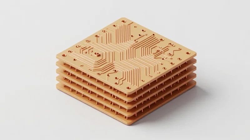
Micro-Via Aspect Ratio Constraints
For high-frame rate AR/VR applications, the aspect ratio (depth-to-diameter) of laser-drilled micro-vias is the critical factor in ensuring reliable copper plating. As thin-core HDI stacks push towards higher density, maintaining a conservative ratio—ideally not exceeding 0.75:1 for production yields—prevents the 'dog-bone' or 'hourglass' plating defects that compromise signal integrity.
| Feature | Standard HDI | High-Speed AR/VR HDI |
|---|---|---|
| Max Aspect Ratio | 1.0:1 | 0.75:1 |
| Via Diameter | 75-100 μm | 50-65 μm |
| Plating Void Risk | Low | High (Requires Pulse Plating) |
Best Practices for Laser Drilling and Plating
Achieving reliable interconnects in thin cores requires a symbiotic relationship between laser parameters and plating chemistry. If the laser pulse energy is too high, it creates excessive heat-affected zones (HAZ) and carbon residues; if too low, it causes irregular hole geometry. Both scenarios increase the likelihood of plating voids in the via barrel.
- How does via geometry impact signal integrity?
Irregular via shapes increase impedance discontinuities, creating reflections that degrade high-frequency signals necessary for high-frame rate display processing. - What role does pulse plating play in DFM?
Pulse plating is essential for high-aspect-ratio micro-vias, as it facilitates more uniform copper distribution within the narrow barrels compared to traditional DC plating. - Why is the HAZ a critical DFM metric?
The heat-affected zone around the via can lead to resin recession and micro-cracking during thermal cycling; optimizing laser frequency minimizes this degradation.
/* Design Rule Check (DRC) for HDI Micro-Vias */
RULE_MICROVIA_RATIO: 0.75;
RULE_MIN_VIA_PAD_OVERLAP: 25um;
RULE_REQUIRED_PLATING_METHOD: 'Pulse_Periodic_Reverse';
Precision Impedance Control Strategies
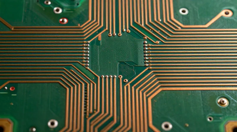
Dielectric Constant (Dk) Stability and Material Selection
In high-density interconnect (HDI) applications, maintaining a 50-ohm signal requires a stable dielectric constant (Dk) across the entire frequency spectrum. For AR/VR displays pushing high frame rates, signal degradation often stems from glass-weave effects, where the local Dk fluctuates between resin-rich areas and glass-fiber-heavy regions. To mitigate this, engineers should specify low-profile copper foils and spread-glass fabric weaves to ensure a homogeneous electromagnetic environment.
Managing Trace Geometry Tolerances
In fine-pitch HDI designs, even minor deviations in trace width—often introduced by non-uniform etching—lead to impedance mismatches. The transition from subtractive etching to semi-additive processes (SAP) is crucial for meeting tight tolerance requirements.
| Parameter | Standard Tolerance | HDI Advanced Tolerance |
|---|---|---|
| Trace Width | +/- 10% | +/- 5% |
| Dielectric Thickness | +/- 10% | +/- 3% |
| Impedance Variance | +/- 10% | +/- 5% |
Frequently Asked Questions
- How does glass-weave effect influence impedance?
The mismatch in Dk between epoxy resin and glass fiber creates a non-uniform field, which causes signal jitter and timing skews that are catastrophic at high-frame-rate display frequencies. - Is back-drilling necessary for HDI impedance control?
While back-drilling is effective, it is often incompatible with ultra-thin HDI cores; instead, blind and buried via structures should be used to minimize signal stubs. - What is the primary benefit of mSAP over subtractive etching?
Modified Semi-Additive Processing (mSAP) enables superior trace definition and vertical sidewall geometry, which significantly reduces impedance fluctuations compared to conventional etching.
Copper Balancing for Mechanical Stability
The Mechanics of Copper Imbalance in HDI Stacks
In the context of high-frame rate AR/VR devices, any physical deviation in the PCB substrate directly impacts the alignment of optical modules and high-speed connectors. Copper acts as a mechanical restraint during the lamination process; asymmetrical distribution creates varying coefficients of thermal expansion (CTE) across the board surface. When copper density is significantly higher on one side of the neutral axis, the material tends to bow or twist during the thermal excursions of reflow soldering, leading to interconnect failure and misalignment of sensitive lens assemblies.
Design Best Practices for Symmetry
- Implement Copper Thieving
Utilize non-functional copper patterns (thieving) in areas with low routing density to equalize the copper-to-dielectric ratio across all signal and plane layers. - Stackup Mirroring
Ensure that your stackup is strictly symmetric relative to the physical center of the PCB, mirroring both the material thickness and copper weight across the core. - Route Balancing
Distribute high-speed signals across multiple layers rather than concentrating routing on a single side, which prevents localized stiffness gradients.
| Parameter | Asymmetric Design Impact | Balanced Design Result |
|---|---|---|
| Board Warping | High risk during reflow | Minimal deviation |
| Optical Alignment | Poor focus repeatability | High precision stability |
| Thermal Stress | Concentrated at interface | Distributed uniformly |
Computational Validation of Copper Distribution
Engineers should utilize EDA tool features to generate a 'Copper Balance Report.' Target a variation of less than 10% in copper coverage between adjacent layers to ensure the internal laminate stresses remain within the elastic limit of the dielectric material. By prioritizing uniform copper distribution early in the layout phase, designers can effectively eliminate the need for costly corrective mechanical stiffeners that would otherwise increase the weight and profile of the wearable device.
Managing Crosstalk in High-Density Routing

In the confined architecture of AR/VR headsets, crosstalk is a primary threat to signal integrity, especially as frame rates climb into the 120Hz-240Hz range. Managing high-speed signals in ultra-compact HDI boards requires moving beyond standard trace-to-trace clearance rules and adopting a more sophisticated approach to return path continuity and electromagnetic coupling.
Differential Pair Spacing and Coupling Optimization
To minimize crosstalk while maintaining density, designers must implement a 'loose vs. tight' coupling strategy based on signal frequency and board thickness. Tighter coupling (S < 2H) improves immunity to external noise but increases the sensitivity to manufacturing tolerances.
| Parameter | Recommended Strategy | Constraint |
|---|---|---|
| Intra-Pair Spacing | Match dielectric height (H) | Maintain +/- 0.5 mil tolerance |
| Inter-Pair Isolation | Minimum 3H spacing | Shield with ground stitching |
| Stitching Via Pitch | Lambda/10 at target frequency | Max 20 mil grid |
Advanced Mitigation FAQ
- How does via stitching reduce crosstalk?
Via stitching effectively creates a Faraday cage effect around high-speed traces, forcing the return current to flow directly underneath the signal path and reducing the loop area. - When is 'back-drilling' necessary?
Back-drilling is essential in multi-layer HDI stacks to remove via stubs, which act as resonant antennae at frequencies exceeding 10GHz, potentially causing significant signal reflection and crosstalk. - Can guard traces replace ground stitching?
Guard traces are generally insufficient for high-density AR/VR PCBs. Ground stitching is superior because it provides a lower-impedance return path that better contains radiated electromagnetic fields.
Ultimately, the combination of controlled coupling and redundant ground stitching ensures that high-bandwidth data remains clean from source to display, preventing visual artifacts in immersive HMD environments.
Surface Finish Selection for Signal Integrity
In high-frame rate AR/VR applications, signals often reach frequencies where the skin effect restricts current flow to the outermost microns of the conductor. Consequently, the surface finish is no longer merely a protective layer but an integral part of the signal path. Selecting a finish with low dielectric loss and minimal surface roughness is essential to minimize insertion loss and avoid signal degradation in high-speed data transmission.
Comparative Analysis of Surface Finishes
| Finish | Signal Integrity Impact | Surface Topography | Primary Application |
|---|---|---|---|
| ENIG | Moderate (Nickel loss) | Very Smooth | General HDI / BGA |
| ENEPIG | Excellent | Very Smooth | High-Frequency RF |
| Immersion Silver | Good | Extremely Smooth | Low-Loss Signal Paths |
Key Considerations for High-Speed HDI
- Why does Nickel pose a risk in high-frequency designs?
Nickel is ferromagnetic and possesses relatively high resistivity. At frequencies exceeding 5GHz, the current tends to penetrate the nickel layer in ENIG, leading to increased insertion loss and potential skin effect-related attenuation. - Is ENEPIG the superior choice for AR/VR?
ENEPIG (Electroless Nickel Electroless Palladium Immersion Gold) is often preferred for high-frame rate boards because the palladium layer acts as a barrier, preventing nickel interaction with the signal while providing a highly stable, planar surface for fine-pitch components. - How does surface roughness correlate to signal loss?
Surface roughness increases the effective path length of the electron flow. Finishes that maintain extreme planarity, such as Immersion Silver, reduce the impact of resistive losses associated with surface irregularities at high GHz ranges.
For HDI designs requiring maximum signal integrity, avoid finishes that introduce significant conductive loss or magnetic barriers. When designing for ultra-high frame rates, prioritize ENEPIG to balance longevity with high-frequency performance, ensuring your DFM protocols account for the electromagnetic influence of the plating stackup.
Thermal Management Through PCB Layout
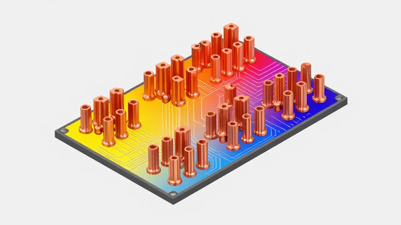
Strategic Thermal Via Placement and Signal Integrity
Thermal management in compact AR/VR devices is inherently constrained by the need to dissipate heat from processors without creating electromagnetic interference or impedance discontinuities. Engineers must utilize 'thermal via farms' positioned directly under high-power components, but these must be optimized for size and spacing to prevent excessive signal coupling. To maintain integrity, implement thermal via stitching using a staggered grid that minimizes the parasitic capacitance introduced to adjacent high-speed differential pairs.
Heat-Sinking Techniques for HDI Density
| Strategy | Implementation Benefit | Signal Integrity Impact |
|---|---|---|
| Copper Pour Islands | Spreads thermal load away from hotspots | Low; if cleared from high-speed traces |
| Buried Thermal Vias | Reduces profile and improves conduction | Moderate; requires precise back-drilling |
| Metal Core Integration | Highest thermal dissipation capacity | High; requires strict return path planning |
Thermal Design FAQs
- How can I avoid impedance drops when using thermal vias near signal lines?
Ensure a minimum clearance of at least three times the trace width between any thermal via and a high-speed signal path to minimize parasitic influence on local reference planes. - Is conductive via filling necessary for AR/VR applications?
Yes, for high-power SoCs, non-conductive epoxy filling can act as an insulator; copper-plated conductive via filling is superior for transferring heat directly to the bottom side of the HDI stack. - Should thermal vias be connected to the ground plane?
Ideally, yes. Connecting thermal vias to the main ground plane provides a dual-purpose path for both thermal dissipation and return current, provided the layout prevents local resonance.
Design for Assembly (DFA) and Inspection
Design for Assembly (DFA) Strategies for HDI PCBs
In the confined space of AR/VR headsets, assembly precision is paramount. DFA for high-density interconnect (HDI) PCBs requires careful consideration of component footprints, clearance, and panelization. To facilitate robotic pick-and-place, maintain a minimum keep-out zone of 0.5mm around all connectors and optical interface components, ensuring clearance for nozzles that could otherwise cause short-circuits or mechanical damage to dense micro-via arrays.
Optimizing AOI and X-Ray Inspection
Advanced HDI designs often feature blind and buried vias that are invisible to optical inspection systems. Implementing robust inspection strategies is essential for verifying multi-layer registration and solder joint integrity.
| Feature | AOI Compatibility Strategy | X-Ray Inspection Benefit |
|---|---|---|
| BGA/CSP Packages | Include high-contrast fiducials for alignment | Essential for void detection and bridging |
| Blind/Buried Vias | N/A (Invisible to AOI) | Verification of copper fill and alignment |
| High-Density SMT | Ensure unobstructed camera clearance | Confirms solder fillet wetting beneath components |
Frequently Asked Questions
- How do copper pour patterns impact AOI accuracy?
Large, unbroken ground planes can cause reflective glare, leading to false negatives during optical inspection. Use cross-hatched copper or matte solder masks to reduce signal noise for AOI sensors. - What are the X-ray requirements for high-frame rate PCBs?
Due to the extreme sensitivity of signal integrity, X-ray inspection must be capable of detecting micro-voids in solder joints that might cause impedance discontinuities or intermittent signal losses at high frequencies. - Why is fiducial placement critical in HDI designs?
In multi-layer HDI boards, fiducials must be present on every layer to assist in registration. Misalignment during the lamination process can lead to via breakout, which is catastrophic for signal integrity.
Successfully shipping AR/VR hardware requires an obsessive focus on DFM at every stage of the design cycle. By prioritizing impedance control, structural stability, and manufacturing precision, you can bridge the gap between concept and high-performance reality. Ready to optimize your next project? Contact our engineering team today for a comprehensive DFM audit of your PCB layout.
