
In the hyper-competitive race to define the metaverse, hardware reliability is the ultimate differentiator. As VR/AR devices shrink in size while growing in computational demand, the printed circuit board (PCB) has become the primary bottleneck for both profit margins and production speed. This analysis explores how strategic High-Density Interconnect (HDI) implementation empowers manufacturers to overcome thermal constraints and complex routing, turning design efficiency into a massive competitive advantage.
The Evolution of Spatial Computing Hardware Requirements
From Prototypes to Performant Wearables
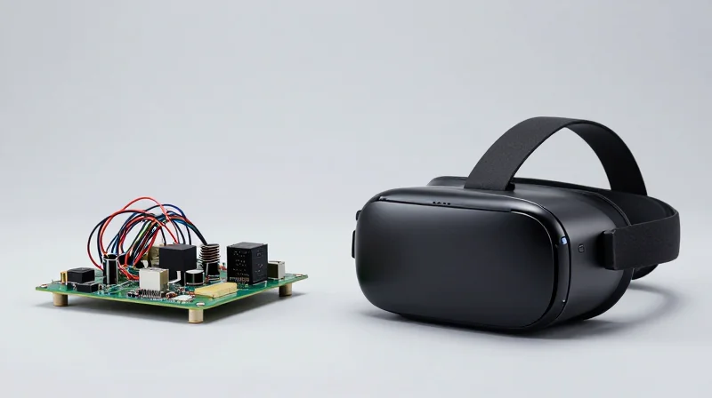
Early spatial computing prototypes were characterized by bulky, inefficient circuit assemblies that prioritized functional testing over form factor. As the industry transitions toward consumer-grade virtual reality headsets, the engineering paradigm has shifted to prioritize aggressive space constraints, thermal management, and high-speed data integrity. This transition necessitates the move from standard rigid boards to advanced HDI PCB architectures capable of supporting higher component densities without compromising structural integrity or user comfort.
Hardware Requirement Evolution Matrix
| Feature | Legacy Prototype | Modern Spatial Hardware |
|---|---|---|
| PCB Technology | Standard Rigid/Multi-layer | HDI (Microvias/Build-up) |
| Component Density | Low/Moderate | Ultra-High |
| Form Factor | Chassis-based | Wearable/Ergonomic |
| Thermal Strategy | Passive/Convection | Integrated Heat Dissipation |
Key Drivers of HDI Adoption
- Why is trace miniaturization critical?
Smaller trace widths and spacing allow for tighter component pitch, which is essential to reduce the overall motherboard surface area in head-mounted displays. - How do microvias impact performance?
Microvias reduce parasitic capacitance and inductance compared to through-hole vias, facilitating the high-speed signal integrity required for 8K resolution and low-latency tracking. - What role does ROI play in HDI selection?
While HDI manufacturing has a higher initial cost per layer, it minimizes board size and reduces the need for secondary daughter boards, ultimately decreasing system-level assembly costs and increasing product reliability.
Understanding the HDI Advantage in Modern Headsets
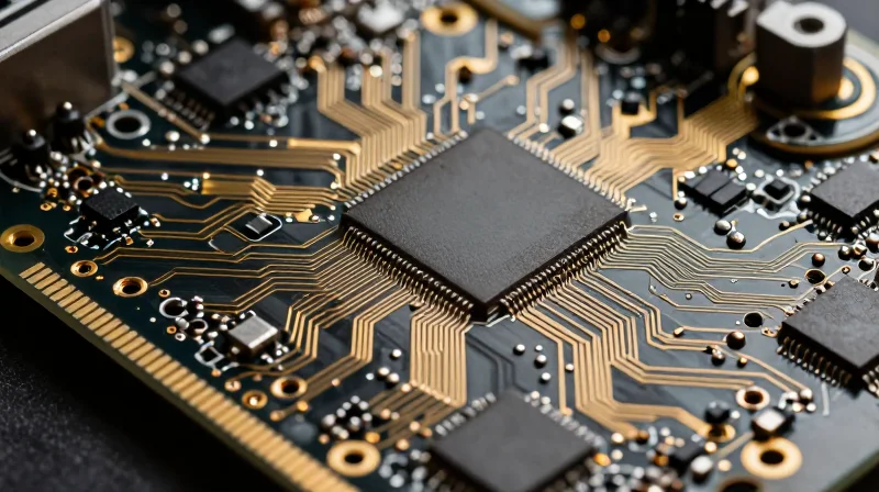
As virtual reality devices evolve from tethered prototypes to untethered, lightweight wearables, the internal hardware architecture must undergo a fundamental transformation. HDI technology serves as the architectural foundation for this shift, moving beyond traditional multi-layer PCB design to incorporate advanced fabrication techniques like laser-drilled micro-vias and extreme fine-pitch surface-mount technology. This approach allows manufacturers to pack high-speed processing and sophisticated sensor arrays into a compact form factor that maintains thermal stability and signal integrity.
The Engineering Mechanics of HDI in VR
The integration of HDI in VR hardware focuses on the elimination of wasted space through 'any-layer' interconnection. By utilizing micro-vias, signal paths are significantly shortened, which is vital for the high-frequency demands of modern spatial optics and ultra-low-latency tracking systems. The increased routing density enables the use of smaller silicon packages, directly supporting the slim profile required for consumer acceptance.
| Metric | Traditional PCB | HDI Technology |
|---|---|---|
| Via Technology | Through-hole | Micro-via (Laser) |
| Component Pitch | Standard (0.5mm+) | Fine-pitch (<0.4mm) |
| Signal Integrity | Moderate (high crosstalk) | Superior (shortened paths) |
| Device Weight | Heavier | Optimized/Minimal |
Frequently Asked Questions
- Why are micro-vias essential for VR?
Micro-vias reduce the 'stub' effect on high-speed traces, preventing signal reflections that can degrade the visual fidelity of 4K or 8K displays in real-time. - Does HDI impact manufacturing costs?
While unit costs for HDI PCBs are higher due to complex layering, the total ROI is optimized by reducing device size, improving energy efficiency, and decreasing the need for additional mechanical cooling solutions. - How does fine-pitch routing assist spatial computing?
Fine-pitch routing allows for the closer integration of IMUs (Inertial Measurement Units) and camera sensors, essential for reducing motion-to-photon latency.
Reducing Device Failure Rates Through Thermal Integrity
Thermal Management Challenges in Compact VR Environments
As VR headsets transition toward lightweight, ergonomic form factors, the integration of high-performance SoCs and sensors into increasingly compact spaces creates immense thermal pressure. In an HDI architecture, the higher density of copper traces and the prevalence of micro-vias decrease the total thermal mass, making conventional cooling methods insufficient. If left unmanaged, localized hot spots accelerate dielectric degradation and increase the likelihood of solder joint fatigue, ultimately driving up warranty costs and reducing overall ROI.
Strategic Thermal Dissipation Techniques
| Strategy | Mechanism | Impact on Reliability |
|---|---|---|
| Thermal Vias | Plated through-holes connecting heat-producing components to inner ground planes. | Reduces junction temperature by facilitating heat spread. |
| Embedded Heat Spreaders | Integration of copper coins or thermal paste within the board stack-up. | Provides a high-conductivity path for passive heat rejection. |
| Material Selection | Utilization of high-Tg (glass transition temperature) laminates. | Prevents board warping and mechanical stress under sustained thermal cycling. |
Improving Reliability Through Design-for-Manufacturing (DFM)
Reducing field failures requires a proactive approach to thermal integrity during the layout phase. By optimizing the distribution of power-intensive components and ensuring symmetric thermal expansion profiles, designers can mitigate the stresses that typically cause interconnect failures in high-density environments.
- How do micro-vias impact thermal reliability?
While micro-vias are essential for HDI, they must be properly stacked or staggered to prevent thermal expansion discrepancies that could cause barrel cracking during extreme temperature fluctuations. - Does higher board density always lead to higher failure rates?
Not necessarily; while higher density increases the potential for thermal bottlenecks, sophisticated simulation and optimized thermal relief patterns allow for smaller, more reliable hardware compared to loosely routed boards. - What is the role of Tg (Glass Transition Temperature) in this context?
Selecting materials with a higher Tg ensures the substrate maintains structural rigidity even when localized temperatures spike, preventing the micro-cracking of vias that leads to premature device failure.
Streamlining Manufacturing Cycles with DFM Optimization
Accelerating Time-to-Market through Proactive DFM
In the fast-paced development cycle of VR hardware, waiting until a prototype is complete to assess manufacturability is a primary cause of ROI erosion. By integrating DFM protocols during the initial stack-up design—specifically focusing on aspect ratios for micro-vias and plating uniformity—engineering teams can avoid the costly 're-spin' cycle. Transitioning to a concurrent engineering model where fabricators provide early feedback on HDI complexity ensures that the design intent is aligned with the specific technical capabilities of the high-volume production facility.
Comparison of Traditional vs. DFM-Optimized HDI Flows
| Variable | Traditional Design Cycle | Optimized DFM Cycle |
|---|---|---|
| Design Iterations | 3-5 Cycles | 1-2 Cycles |
| Tooling Lead Time | Extended | Minimized |
| Assembly Yield | Low to Moderate | High (Target >98%) |
| Fabricator Feedback | Post-Submission | Pre-Submission |
Strategic Optimization for High-Volume VR Assemblies
- How does via-in-pad technology impact assembly speed?
Implementing via-in-pad (VIPPO) allows for tighter component placement, but requires precision planarization during fabrication. Optimizing this at the design stage reduces solder voiding and improves pick-and-place accuracy, drastically increasing assembly throughput. - What is the primary role of panelization in HDI cost control?
Optimizing panel utilization (the 'nesting' of PCBs on a manufacturing substrate) directly reduces material waste. For complex VR headset boards, effective panelization can improve material yield by up to 20%, significantly lowering the per-unit BOM cost. - How do copper balance requirements affect cycle time?
Uneven copper distribution causes board warping during lamination. Standardizing copper density across layers early in the DFM process prevents structural defects, ensuring that the production line avoids stoppages due to warped substrates.
To achieve maximum ROI, firms must treat DFM not as a final validation gate, but as a continuous thread throughout the CAD/CAM integration phase. Establishing design rules that account for the limitations of laser drilling for HDI micro-vias early in the process creates a predictable manufacturing path, ensuring that high-density VR headsets move from the prototype phase to consumer-grade mass production with minimal friction.
Signal Integrity and Routing Efficiency

Mitigating High-Frequency Signal Degradation
In the dense physical constraints of VR headsets, high-speed differential pairs are susceptible to electromagnetic interference (EMI) and signal attenuation. Maintaining signal integrity requires precise control over trace impedance and dielectric constant stability. By leveraging HDI stack-up strategies, engineers can utilize shorter routing paths and micro-via transitions that effectively minimize parasitic capacitance, ensuring that high-bandwidth signals—such as those powering 4K-per-eye displays—remain crisp and latency-free.
Routing Efficiency vs. Signal Integrity
| Strategy | Signal Integrity Impact | Routing Efficiency Gain |
|---|---|---|
| Staggered Micro-vias | High: Reduced stub length | Medium: Requires more surface area |
| Any-Layer HDI | Highest: Direct signal routing | Highest: Maximizes internal layer utility |
| Buried Vias | Medium: Potential impedance mismatch | High: Frees up external layer routing |
Advanced Stack-up Tactics for Crosstalk Reduction
Crosstalk remains the primary adversary of high-density VR boards. Implementing 'Ground-Signal-Signal-Ground' (GSSG) configurations and optimizing the reference plane distance are essential. Utilizing advanced core materials with lower dielectric loss tangents helps preserve signal power over longer traces, further enhancing the ROI by reducing the need for costly signal repeaters or active re-timers.
Frequently Asked Questions
- How do micro-vias improve signal performance?
Micro-vias reduce parasitic inductance and capacitance compared to through-hole vias by shortening the electrical path and eliminating long stubs that cause signal reflections. - Does higher density always lead to higher crosstalk?
Not necessarily; while physical proximity increases, advanced routing topologies and optimized reference planes in HDI designs allow for better isolation and controlled return paths, which actually improve signal stability.
Cost Analysis: High-Density Interconnect vs. Standard Fabrication
The Economic Trade-Off: Upfront Investment vs. Long-Term Value
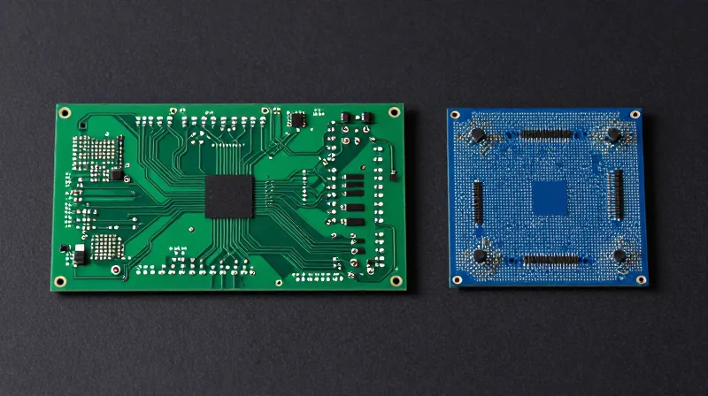
While HDI fabrication demands a higher unit cost due to laser drilling, microvias, and sequential lamination, it provides a superior path to Return on Investment (ROI) for VR hardware. By shrinking board real estate and reducing layer counts, HDI designs inherently lower the raw material consumption and volume requirements for high-performance enclosures. Strategic adoption of HDI effectively offsets its premium pricing through increased product miniaturization and significantly reduced field failure rates.
| Cost Variable | Standard Fabrication | HDI Fabrication |
|---|---|---|
| Unit Fabrication Price | Low | High |
| Material Efficiency | Moderate | Very High |
| Routing Complexity | High | Low |
| Field Failure Risk | Higher | Lower |
| Product Weight/Size | Larger | Optimized |
Strategic Cost Considerations
- How does layer count impact ROI?
HDI allows for higher component density on fewer total layers. Reducing a board from 12 layers to 8 through HDI implementation can offset the per-layer cost premium by reducing lamination cycles and material waste. - Do assembly costs change with HDI?
Yes, HDI simplifies assembly by enabling finer pitch components and integrated via-in-pad technology, which reduces solder bridge risks and rework cycles, ultimately accelerating high-volume throughput. - What is the hidden cost of traditional boards in VR?
Traditional fabrication in high-density VR designs often requires complex fan-out schemes that increase trace length, leading to signal degradation. The cost of 'fixing' these signal issues in later iterations often exceeds the initial investment of HDI.
To achieve optimal ROI, engineering teams must transition from viewing HDI as a 'premium' expense to recognizing it as a 'system-wide' efficiency tool. By investing in early-stage HDI design, manufacturers mitigate the risks of expensive board redesigns and excessive inventory churn caused by component obsolescence or reliability issues in compact VR headsets.
Supply Chain Resilience and Scalability
Strategic Scaling from Prototyping to Mass Production
The transition from low-volume pilot programs to full-scale mass market manufacturing is where many VR hardware projects fail due to design rigidity. By prioritizing design-for-scalability early in the lifecycle, engineers can avoid the common pitfalls of locked-in proprietary material chains and process-sensitive geometries that increase yield losses during high-volume production.
Strategies for Supply Chain Resilience
- Multi-Source Material Qualification
Design your HDI stack-up around industry-standard dielectric constant (Dk) and dissipation factor (Df) values to ensure that multiple board houses can meet your signal integrity requirements without requiring a complete redesign. - Panelization Efficiency
Work with fabrication partners early to optimize PCB layout for standard panel sizes, reducing material waste and lowering per-unit costs as production volumes ramp up. - Lead-Time Risk Mitigation
Avoid over-reliance on specialized micro-via technologies that may be limited to specific vendors; instead, use robust, high-yield via-in-pad structures that are widely supported by tier-one and tier-two manufacturers.
Comparative Analysis: Scalability Drivers
| Scalability Factor | Legacy/Rigid Approach | Resilient HDI Strategy |
|---|---|---|
| Material Sourcing | Single-source proprietary laminates | IPC-standardized high-speed materials |
| Via Technology | Extreme micro-vias (<50um) | Standardized stacked/staggered vias |
| Manufacturing Base | Locked to specific factory capabilities | Designed for multi-vendor compatibility |
| Yield Management | High sensitivity to process variations | Wide manufacturing tolerance windows |
Finally, integrating automated optical inspection (AOI) data feedback loops during the pilot phase is critical for ROI. By establishing a digital thread between PCB CAD data and manufacturer yield metrics, engineering teams can proactively adjust design tolerances before entering the mass-market phase, ensuring high quality remains consistent regardless of the scale.
Case Study: Achieving Faster Time-to-Market
Overcoming the Iteration Bottleneck
For a tier-one VR developer struggling with thermal management and signal density in a prototype headset, the transition from traditional rigid boards to a multi-stage HDI (Any-Layer) stack-up proved transformative. By integrating micro-vias and buried capacitance within a tighter footprint, the engineering team bypassed the need for multiple redesigns caused by routing congestion, effectively accelerating the path from proof-of-concept to final validation.
Development Lifecycle Comparison
| Development Phase | Standard Fabrication (Weeks) | Integrated HDI Approach (Weeks) |
|---|---|---|
| Board Layout & Routing | 8 | 5 |
| Design Rule Checking | 4 | 2 |
| Prototyping & Iterations | 12 | 6 |
| Final Validation | 6 | 4 |
Key Lessons in Accelerated Deployment
- How did HDI integration impact routing efficiency?
The use of laser-drilled micro-vias allowed for 'via-in-pad' technology, which liberated significant real estate on inner layers and eliminated the need for complex, time-consuming serpentine traces. - What was the primary driver of faster market entry?
Early adoption of HDI allowed for parallel signal and power integrity simulation, reducing the mechanical interference conflicts that typically plague late-stage prototype assembly. - Did upfront investment pay off?
While initial fabrication costs were 20% higher than traditional methods, the reduction in iteration cycles saved an estimated $450k in development overhead and allowed the product to hit the holiday launch window.
Ultimately, the case study demonstrates that HDI is not merely a space-saving tool for VR hardware; it is a strategic asset for compressing the development timeline. By mitigating signal integrity risks early, firms can move beyond reactive design fixes and focus on delivering high-fidelity immersive experiences to the end-user faster than competitors.
Optimizing your PCB layout is no longer just a technical necessity; it is a critical business strategy that dictates your ability to scale profitably in the VR market. By embracing high-density interconnects, you protect your bottom line and ensure a premium user experience that stands the test of time. Ready to refine your hardware production strategy? Contact our engineering team today to audit your current designs for maximum manufacturing efficiency.
