
In the competitive consumer appliance market, the reliability of your air purifier hinges on its controller board. As systems become more compact and packed with sensor arrays, engineers face dual challenges: electromagnetic interference and thermal saturation. This guide provides actionable DFM strategies to bridge the gap between prototype perfection and large-scale manufacturing success.
Understanding the Air Purifier Controller Ecosystem
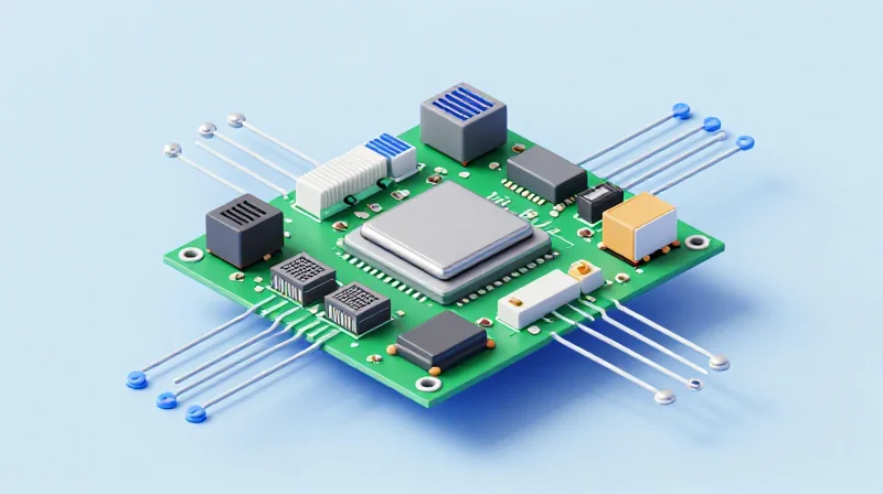
Core Architectural Pillars of Air Purifier Controllers
A high-performance air purifier controller is the nexus of environmental monitoring, airflow regulation, and user interface management. Achieving design reliability requires a deep understanding of the interactions between analog sensor inputs, digital processing units, and high-voltage power switching components.
| Component Category | Functional Role | DFM Critical Factor |
|---|---|---|
| Sensors | PM2.5, VOC, Temperature/Humidity | Signal noise immunity and trace isolation |
| Motor Control | BLDC/AC Motor Pulse Width Modulation | Heat dissipation and EMI suppression |
| Power Management | AC/DC conversion and regulation | Creepage and clearance compliance |
| UI/Connectivity | LEDs, Displays, WiFi/BLE modules | Antenna placement and RF interference |
Key Design Considerations for Integrated Systems
- How does sensor integration impact PCBA layout?
Sensitive air quality sensors are prone to noise from digital circuits; designers must implement dedicated analog ground planes and keep sensor signal traces short to avoid EMI corruption. - What are the primary motor control challenges?
Driving BLDC motors necessitates high-current paths that can induce significant switching noise. Proper component placement for gate drivers and adequate copper weight are essential to prevent trace burnout and thermal hotspots. - How is safety managed in the power architecture?
Due to the presence of high-voltage AC mains, strict adherence to IPC-2221 spacing rules is required for creepage and clearance to ensure product safety and compliance with global regulatory standards.
To ensure long-term reliability in high-performance units, DFM strategies must focus on thermal management for high-load components and robust signal integrity for sensor data. Implementing comprehensive test points during the board design phase allows for streamlined production testing and faster fault isolation during assembly.
Advanced EMI Shielding Techniques

Strategic Ground Plane Segmentation
Effective EMI mitigation begins with rigorous ground plane isolation. For air purifier controllers, which mix low-voltage digital sensors with high-current PWM motor controllers, physical separation of Analog Ground (AGND) and Digital Ground (DGND) is mandatory. These planes should remain isolated across the entire stack-up, connected only at a single, well-defined star ground point near the primary power supply entry to prevent return path cross-talk.
Implementation of Physical Shielding Cans
Physical shielding cans are essential for isolating high-frequency switching regulators or wireless communication modules. When integrating these components, ensure that the PCB footprint includes a continuous perimeter ground trace to facilitate solder-reflow attachment of the shield. Designers must also ensure adequate clearance between internal components and the shield wall to prevent short circuits and parasitic capacitance.
| Shielding Strategy | Target Noise Source | DFM Consideration |
|---|---|---|
| Faraday Cans | Wireless/RF Modules | Requires low-impedance ground vias |
| Ferrite Beads | High-Frequency Switching | Must match peak impedance to noise freq |
| Plane Isolation | Motor PWM Noise | Avoid trace routing over plane splits |
EMI Shielding Best Practices FAQ
- How do you manage vias near shield walls?
Place stitching vias at a maximum pitch of 1/20th of the wavelength of the highest noise frequency to ensure a low-impedance path to ground. - Should shielding cans be grounded?
Yes, they must be tied to the chassis or system ground via a dedicated trace that is isolated from sensitive analog signals to prevent noise injection. - Why avoid routing traces over split ground planes?
Routing over a split creates a loop antenna effect, drastically increasing radiated emissions and causing significant EMI compliance failure.
Precision Thermal Management Strategies
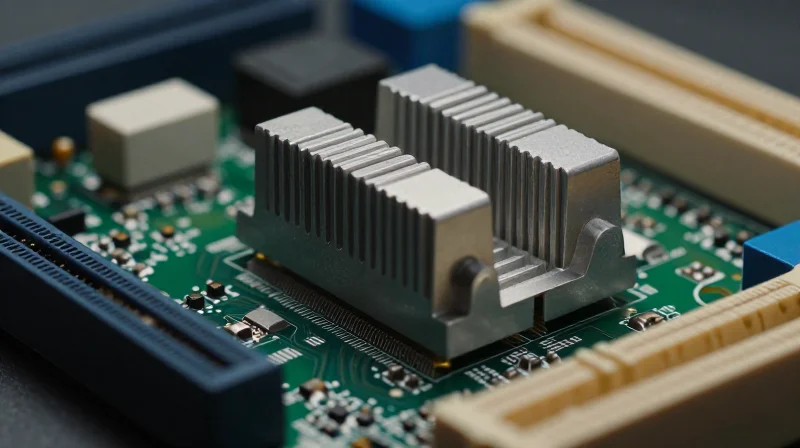
Precision Thermal Management Strategies
High-performance air purifier controllers demand precise thermal management to ensure the longevity of high-power brushless DC (BLDC) motor drivers and high-speed microcontrollers. By integrating effective thermal dissipation paths directly into the PCBA architecture, designers can prevent thermal throttling, minimize component drift, and extend the mean time between failures (MTBF) under continuous duty cycles.
Optimizing Thermal Dissipation Path
Effective heat management relies on a low-thermal-resistance path from high-power components to the board's substrate. For surface-mount high-power components, the primary interface is the thermal pad, which must be connected to internal copper layers via an array of stitched thermal vias.
| Strategy | Implementation Rule | Thermal Impact |
|---|---|---|
| Thermal Vias | 0.3mm diameter on 0.8mm grid | High thermal conductivity to inner planes |
| Copper Pour | Minimum 2oz weight for high power | Increased surface area for heat dissipation |
| Component Spacing | Maintain >10mm from heat-sensitive ICs | Reduced secondary thermal heating |
Frequently Asked Questions on Thermal Design
- How does copper weight influence PCBA thermal performance?
Heavier copper weights (2oz or higher) significantly reduce the thermal resistance of the PCB substrate, allowing the board itself to act as a heat spreader, which is critical for motor drivers. - What is the recommended approach for thermal via placement?
Thermal vias should be placed directly under the component's exposed thermal pad and stitched to the largest available ground plane to maximize heat distribution across the PCB layers. - Can solder mask impact thermal performance?
Yes, maintaining a 'solder mask defined' area over heat-dissipating copper is often preferred to ensure a uniform thermal interface without the insulating effects of excessive mask material.
DFM Rules for High-Volume Assembly Efficiency
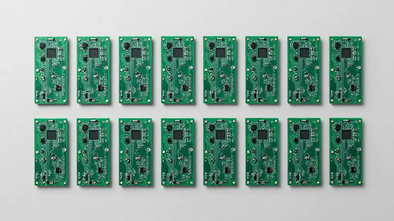
Standardizing Footprints and Panelization
High-volume assembly relies on repeatability. For air purifier controllers, establishing IPC-7351B compliant footprints ensures consistent solder paste release and fillet formation. Standardizing pad geometries across the board allows pick-and-place machines to operate with tighter tolerances, significantly reducing the probability of component tombstoning or bridging during reflow.
| Parameter | Recommended Practice | Impact on Production |
|---|---|---|
| Panelization | V-score with break-away tabs | Reduces stress-induced micro-cracking |
| Fiducials | 3 per board, 1mm diameter | Ensures precise optical alignment |
| Component Spacing | Minimum 0.5mm clearance | Prevents solder bridges in high-speed lines |
Optimizing Throughput for Automated SMT
To achieve peak efficiency, design for the assembly line, not just the schematic. Implementing fiducial marks on both the main panel frame and individual circuit units allows for local compensation of board warping, which is essential when dealing with the high-thermal mass of power-heavy air purifier boards.
- Why are fiducial marks critical for automation?
Fiducials serve as primary reference points for vision systems, enabling the pick-and-place machine to accurately align components despite variations in board manufacturing or expansion during reflow. - How does panel size affect throughput?
Balancing panel size is a trade-off; larger panels increase yield per cycle but can cause board sagging. For most controller boards, a 250mm x 300mm panel is optimal for maintaining rigidity. - What is the role of solder mask dams?
Solder mask dams between closely spaced pads are essential to prevent solder bridging, especially on fine-pitch microcontrollers used in sensor-heavy air purifier designs.
Component Selection for Reliability and Availability
Strategic Sourcing and Component Lifecycle Management
To maintain high availability in air purifier production, designers must prioritize components with long lifecycles and high multi-source availability. Selecting 'End-of-Life' (EOL) prone parts, especially for microcontrollers (MCUs) and power management ICs (PMICs), creates significant risk for production bottlenecks. Designers should implement a 'Preferred Parts List' (PPL) that mandates components with verified secondary sources and robust stock depth.
| Component Category | Reliability Metric | Availability Strategy |
|---|---|---|
| Microcontrollers | Automotive Grade (AEC-Q100) | Commit to 5+ year roadmap |
| Power MOSFETs | Low RDS(on) Thermal stability | Verify dual-vendor footprints |
| Electrolytic Caps | Long-life (10k+ hours @ 105C) | Specify standard case sizes |
Mitigating Risks in the High-Performance PCBA
- Why should you avoid custom ASIC parts?
Custom parts create single points of failure. High-volume PCBA manufacturing relies on standard, commodity-off-the-shelf components that can be swapped without extensive redesign if a supplier faces a shutdown. - How does component density impact availability?
Using ultra-small packages (0201 or smaller) increases pick-and-place precision requirements, which may limit the number of contract manufacturers capable of assembling your board, thereby narrowing your supply chain options. - What role does moisture sensitivity play?
Selecting components with high Moisture Sensitivity Levels (MSL) complicates production schedules by requiring mandatory bake-out times and strict vacuum sealing, slowing down throughput and increasing defect risk.
Ultimately, the selection process must integrate design-for-procurement. By standardizing component footprints and prioritizing high-availability parts, you reduce the 'Design-to-Assembly' cycle time and ensure that your air purifier controller maintains consistent performance throughout its entire product lifecycle.
Designing for Environmental Durability
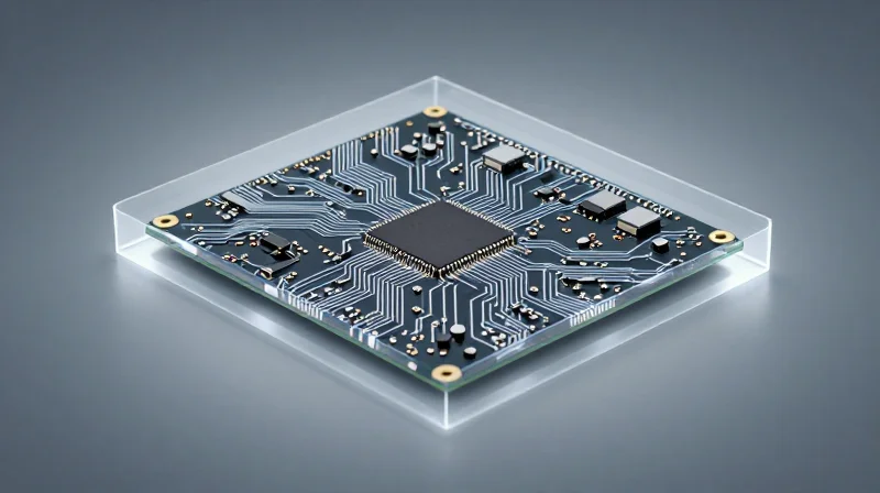
Mitigating Humidity and Contaminant Risks
Air purifiers operate in environments where moisture, dust, and VOC-laden air can quickly degrade unshielded PCBAs through electrochemical migration or corrosion. Advanced DFM for durability centers on implementing robust conformal coating strategies and board-level shielding that isolate sensitive control circuitry from environmental stressors while maintaining necessary thermal performance.
Conformal Coating Selection Strategies
| Coating Type | Moisture Resistance | Ease of Rework | Thermal Performance |
|---|---|---|---|
| Acrylic (AR) | Good | Excellent | High |
| Polyurethane (UR) | Excellent | Difficult | Moderate |
| Silicone (SR) | Excellent | Difficult | High |
| Parylene (XY) | Superior | Impossible | Moderate |
Best Practices for Environmental Reliability
- How does PCB layout impact coating effectiveness?
Avoid high-profile components grouped too tightly, as this creates 'shadow areas' where coating liquid cannot penetrate, leading to thin spots vulnerable to moisture ingress. - What are the common pitfalls in masking during coating?
Ensure connectors, buttons, and thermal pads are accurately masked; improper masking often leads to high-resistance contact points or thermal conductivity failures. - Should I use underfill for high-vibration scenarios?
If the air purifier fan introduces significant vibration, use underfill for BGA or large SMT components to prevent solder joint fatigue, as vibration can crack conformal coatings and open paths for humidity.
Design Guidelines for Corrosion Resistance
1. Keep high-voltage traces spaced at least 2.5mm apart to prevent dendritic growth in humid conditions.
2. Apply liquid-tight gaskets or potting for high-exposure humidity sensors.
3. Implement gold-plated (ENIG) surface finishes to inhibit oxidation compared to traditional HASL finishes.
4. Ensure all test points are located away from edge connectors to minimize ingress risks.
Quality Assurance and Testing Protocols
In-Circuit Testing (ICT) Strategy
ICT serves as the primary mechanism for verifying the structural integrity of the populated PCBA. By utilizing a 'bed-of-nails' fixture, manufacturers can perform precise resistance, capacitance, and diode junction checks to identify short circuits, open traces, or incorrectly oriented components immediately following the soldering process.
Functional Testing (FCT) Protocols
While ICT validates the assembly, FCT mimics the operational environment of the air purifier. By simulating inputs such as fan speed control signals, sensor feedback loops (particulate matter, VOCs), and power management routines, FCT confirms that the microcontroller and peripheral components function as an integrated system under real-world logic parameters.
| Feature | ICT (In-Circuit Testing) | FCT (Functional Testing) |
|---|---|---|
| Primary Goal | Assembly verification | System performance verification |
| Key Metric | Component values/connectivity | Input/Output logic response |
| Detection Focus | Solder bridges, missing parts | Logic failures, firmware bugs |
| Cost Impact | Lower per-unit, high fixture cost | Higher complexity, comprehensive coverage |
Testing Strategy FAQ
- How does ICT design impact PCB layout?
Designers must incorporate dedicated test points on non-critical nets, ensuring they are placed on a standard grid with sufficient clearance from components to accommodate fixture probes without risking solder mask damage. - When is FCT most effective in the production line?
FCT should follow ICT; it is the final gate-check before final housing assembly, ensuring that only boards meeting all performance specifications are committed to the expensive final enclosure. - Can FCT replace ICT entirely?
Generally no, as FCT struggles to isolate individual component failures on complex boards, whereas ICT quickly identifies the exact location of assembly errors.
Scaling from Pilot to Mass Production
Strategic Scaling: From Prototype to Production
Successful scaling hinges on shifting the focus from functional verification to process repeatability. Designers must audit the Bill of Materials (BOM) for single-source dependencies and optimize physical layout features that facilitate high-speed automated assembly, such as panelization strategy and fiducial placement accuracy.
Critical DFM Transitions
| Feature | Pilot Phase | Mass Production Phase |
|---|---|---|
| Components | Performance-centric (Single Source) | Cost-optimized (Multi-sourced/Approved) |
| Panelization | Small panels or individual | Optimized array (high utilization) |
| Testing | Manual Bench testing | Automated ICT/FCT fixtures |
| Documentation | Baseline Gerber files | Controlled ODB++ with PCN process |
Manufacturing Efficiency FAQs
- How does panelization impact yield?
Proper panelization minimizes waste and allows for consistent solder paste application across all units, ensuring uniform board thermal profiles during reflow. - What is the importance of Product Change Notifications (PCN)?
Establishing a formal PCN process ensures that any necessary changes to components or processes during production are tracked, validated, and documented to prevent unforeseen field failures. - When should I transition from ICT to AOI?
Automated Optical Inspection (AOI) should be integrated early for solder joint verification, while ICT is deployed during mass production to confirm electrical parameter integrity at high volume.
To finalize the transition, conduct a Design for Manufacturing (DFM) review specifically focused on assembly speed. Ensure that all SMDs are orientated to minimize nozzle changes on Pick-and-Place machines, and utilize standard surface finishes like ENIG or HASL to keep production costs predictable and procurement lead times consistent.
By integrating rigorous EMI shielding and thermal management into your initial design phase, you significantly reduce the risk of failure in the field and minimize costly rework on the production line. Ready to optimize your air purifier PCBA manufacturing? Contact our engineering team today to audit your design for manufacturing readiness.
