
In the high-stakes world of Uninterruptible Power Supply (UPS) systems, failure is not an option. As power densities rise, standard PCB manufacturing guidelines often fall short, leading to thermal runaway and premature component degradation. This guide explores the critical DFM principles necessary to engineer boards that survive the harshest power environments.
Understanding the High-Current Design Paradigm
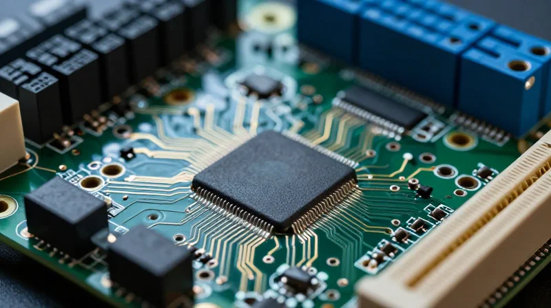
The High-Current Design Paradigm
Designing PCBs for uninterruptible power supply (UPS) systems demands a departure from general-purpose consumer electronic fabrication standards. In high-reliability power electronics, the paradigm shifts from managing simple signal paths to mitigating the physical stresses of extreme current densities, potential hot-spot formation, and the risk of catastrophic dielectric breakdown.
Why Standard DFM Rules Fail
Standard Design for Manufacturing (DFM) guidelines are typically optimized for cost-effective mass production of low-power logic boards. When applied to high-current UPS designs, these general rules overlook the non-linear relationship between copper temperature and material degradation. Ignoring these factors leads to latent failures, such as micro-cracking in plating or localized delamination.
| Parameter | Consumer Electronics Rule | High-Reliability UPS Rule |
|---|---|---|
| Copper Thickness | 0.5 - 1.0 oz | 2.0 - 4.0 oz or heavy copper |
| Trace Spacing | Minimum clearance for signal | Calculated creepage/clearance for HV |
| Thermal Vias | Standard grid | Copper-filled, high-density arrays |
| Substrate | FR-4 standard TG | High-TG or Ceramic-filled |
Critical Considerations for Power Integrity
- How does current density affect trace reliability?
High current density induces Joule heating, which causes thermal expansion. If the coefficient of thermal expansion (CTE) of the copper and substrate are not tightly managed, cyclical thermal loading leads to mechanical fatigue at the copper-to-vial interface. - Why is dielectric strength critical in power stages?
UPS power conversion stages often involve high DC link voltages. Standard spacing rules may suffice for signal integrity but fail to prevent arc tracking or corona discharge, necessitating advanced clearance and creepage analysis.
Optimizing Copper Weight and Trace Width
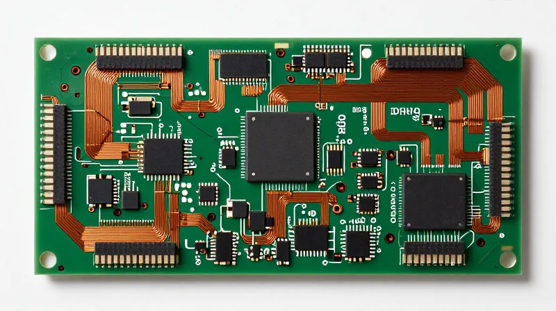
The Physics of Copper Weight and Current Capacity
In high-reliability UPS applications, trace resistance is the primary driver of board-level heat generation. Selecting the appropriate copper weight (typically 2oz to 4oz for power paths) is not merely a matter of current capacity; it is a critical thermal management strategy. Engineers must adhere to the IPC-2152 standard rather than outdated IPC-2221 formulas to calculate the allowable temperature rise for a given cross-sectional area, ensuring the board operates safely under maximum load conditions.
Copper Weight Selection Guidelines
| Copper Weight | Typical Application | Thermal Benefit |
|---|---|---|
| 1 oz (35 µm) | Control/Signal paths | Standard heat dissipation |
| 2 oz (70 µm) | Primary Power Rails | Reduced resistive drop |
| 3+ oz (105 µm+) | High-Current FET/Bus paths | Maximum thermal mass |
Trace Geometry and Aspect Ratio Best Practices
When defining trace widths for high-reliability boards, the copper thickness dictates the minimum etch compensation required. Excessive width can lead to routing congestion, while insufficient width creates localized hot spots. To maintain signal integrity and thermal stability, designers must prioritize short, wide traces for power delivery to minimize inductive losses and resistive heating.
- Why should I avoid using legacy IPC-2221 calculators?
IPC-2221 is widely considered overly conservative and does not account for modern board substrates or the thermal effects of surrounding components, often leading to wasted space and over-designed boards. - How does copper plating variation impact reliability?
Manufacturing tolerances can lead to thinner copper at the edges of a trace. Reliability designs must specify a minimum finished copper weight to ensure the current-carrying capacity is maintained across the entire production lot. - What is the impact of via-in-pad on thermal management?
Placing thermal vias directly in pads under high-current components helps sink heat into inner ground planes, significantly reducing the thermal resistance from the component junction to ambient air.
Thermal Relief and Heat Dissipation Strategies
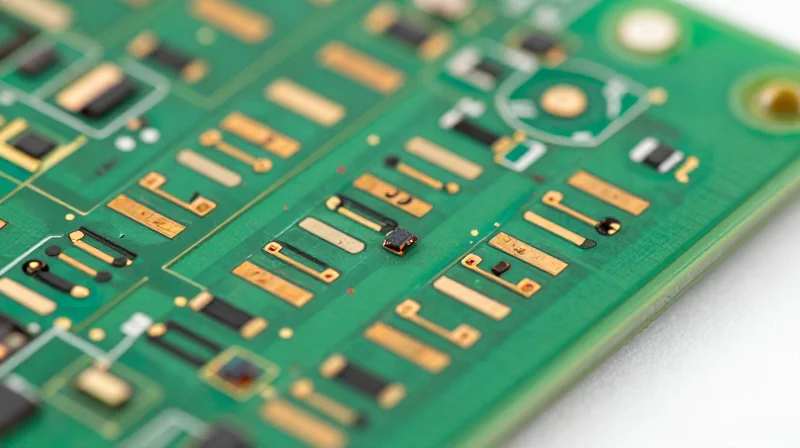
Strategic Implementation of Thermal Relief Patterns
Thermal relief patterns are essential for high-current UPS PCBs to prevent excessive heat sinking during the wave soldering process, which could otherwise lead to cold solder joints. By using spoke-like connections for components tied to large copper planes, designers ensure the assembly process is efficient while maintaining the electrical connectivity required for power distribution.
Design Best Practices for Thermal Relief
- Spoke Geometry Optimization
Utilize at least four spokes for high-current nodes to minimize impedance while maintaining necessary thermal resistance. - Thermal Isolation
Ensure non-electrically active thermal vias are placed near power transistors to facilitate heat transfer from the junction to the internal ground planes. - PCB Fabrication Constraints
Consult with board houses on the minimum spoke width; undersized spokes under high current loads can lead to unintended fuse-like failures.
Heat Dissipation Comparison: Thermal Vias vs. Heatsinks
| Method | Primary Application | Thermal Advantage | Complexity |
|---|---|---|---|
| Thermal Vias | DIP/SMD Power Components | Excellent PCB-to-Plane conduction | Low |
| External Heatsinks | High Power MOSFETs | Efficient convection to ambient | High |
| Copper Pouring | High-Current Traces | Increased surface area for radiation | Low |
Addressing Thermal Cycling Fatigue
UPS systems often undergo rapid thermal cycling, leading to CTE (Coefficient of Thermal Expansion) mismatch issues. To combat this, minimize the copper area directly under surface-mount power components. Over-plating thermal pads can create rigid, brittle solder joints that fracture under cycling; instead, use balanced copper distributions to distribute mechanical stress across the board surface evenly.
Material Selection for Harsh Environments
In high-reliability Uninterruptible Power Supply (UPS) applications, the dielectric material acts as the fundamental barrier against thermal degradation. Standard FR-4 materials often fail to withstand the continuous operating temperatures and rapid thermal cycling inherent in high-power conversion. Engineers must transition to high-glass transition temperature (high-Tg) substrates and metal-core materials to prevent delamination, board warping, and dielectric breakdown.
Substrate Material Comparison
| Material Class | Tg (°C) | Thermal Conductivity | Recommended Use Case |
|---|---|---|---|
| Standard FR-4 | 130-140 | Low | Low-power control logic only |
| High-Tg FR-4 | 170-185 | Moderate | General power stages/High-rel industrial |
| Ceramic-Filled Laminates | 200+ | High | Extreme thermal density/Heat dissipation |
Key Considerations for Material Selection
- Why is the Glass Transition Temperature (Tg) the primary metric?
Tg defines the point where the polymer matrix changes from a rigid state to a rubbery state. Operating near or above this value leads to excessive Z-axis expansion, which frequently cracks plated-through-holes (PTHs). - How does Coefficient of Thermal Expansion (CTE) impact reliability?
CTE mismatch between the copper traces and the substrate causes mechanical stress during heat-up cycles. Low-CTE laminates are essential to preserve the structural integrity of via barrels in high-current power paths. - When should Metal Core PCBs (MCPCBs) be prioritized?
When power density reaches a point where standard dielectric heat spreading is insufficient, MCPCBs provide an aluminum or copper base to act as a heat sink, significantly improving Mean Time Between Failures (MTBF).
For designs involving high-frequency switching MOSFETs or IGBT modules, selecting a material with a stable Dielectric Constant (Dk) and low Dissipation Factor (Df) is equally vital. This ensures that the thermal stability of the substrate does not drift, which would otherwise lead to parasitic signal distortion and electromagnetic interference (EMI) issues in high-reliability UPS infrastructure.
Maintaining Signal Integrity Near Power Planes
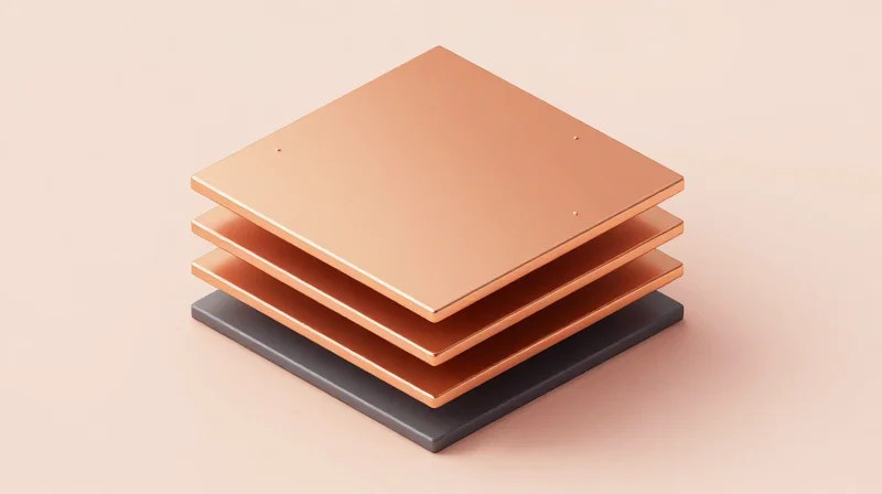
Maintaining Signal Integrity Near Power Planes
In high-reliability UPS systems, maintaining signal integrity requires meticulous stackup design to decouple high-speed control logic from the significant electromagnetic interference (EMI) generated by high-current switching nodes. The objective is to contain the return currents of critical traces to avoid inducing parasitic noise into sensitive analog or logic paths.
Strategic Layer Stackup and Grounding
The most effective method for decoupling is the implementation of a dedicated reference plane strategy. By placing a solid ground plane immediately adjacent to signal layers, you provide a low-impedance return path that restricts loop areas. Avoid routing signals across discontinuities or splits in the ground plane, as these create high-impedance paths that facilitate radiation and crosstalk.
| Strategy | Implementation Benefit | Design Constraint |
|---|---|---|
| Solid Reference Planes | Reduces EMI/RFI emission | Must avoid plane splits |
| Stitching Vias | Provides continuous return path | Increases layer count |
| Trace Separation | Minimizes cross-talk | Increases board area |
Best Practices for Power Noise Mitigation
- Why should high-current switching traces be isolated from logic planes?
Switching nodes often feature fast rise/fall times (high dV/dt), which can induce capacitive coupling into adjacent control signals, potentially triggering false state changes. - How does via stitching help near power planes?
Via stitching connects separate ground planes, ensuring a low-inductance return path for signals that change reference layers, thereby reducing the loop area. - What is the 'Rule of Three' for trace clearance?
Maintain a minimum distance of three times the dielectric height between signal traces and the edges of power planes to prevent edge-effect noise coupling.
/* Design Rule Recommendation */
DFM_Constraint: Clear_Power_Planes = 3 * Dielectric_Thickness;
DFM_Constraint: Via_Stitching_Pitch = 10mm;
Avoid: Routing_Over_Split_Planes = TRUE;
Advanced Via Stitching and Thermal Vias
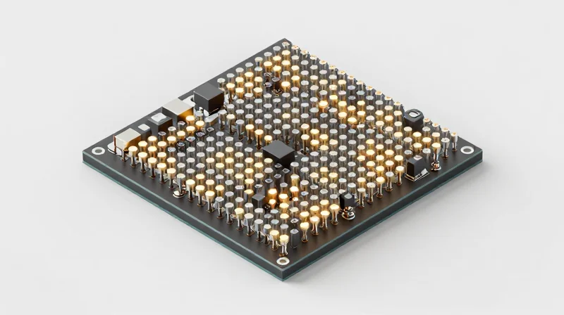
In high-reliability uninterruptible power supply (UPS) PCBs, via stitching and thermal vias are not merely structural elements but essential components for thermal management and signal return path integrity. Proper implementation minimizes parasitic inductance, ensures uniform current distribution, and effectively couples high-power components to internal ground planes for superior heat sinking.
Optimizing Thermal Via Arrays
Thermal via arrays must be designed to balance thermal conductivity with the manufacturing constraints of the PCB fabrication process. To maximize heat transfer from power semiconductor junctions to internal copper planes, utilize a dense grid pattern while maintaining appropriate drill-to-copper clearances to prevent wicking and potential solder voiding.
| Design Parameter | Recommended Practice for UPS | Impact on Performance |
|---|---|---|
| Via Diameter | 0.2mm to 0.3mm | Balances thermal mass and drilling reliability |
| Grid Pitch | 0.5mm to 0.8mm (center-to-center) | Prevents solder starvation and optimizes plane copper |
| Plating Thickness | 25um minimum | Ensures structural integrity during thermal cycling |
Via Stitching for Signal and Power Integrity
Stitching vias are critical for maintaining low-impedance return paths and preventing EMI in switching power stages. By placing stitching vias along the edges of high-frequency signal traces and at the perimeter of large power planes, you effectively reduce common-mode noise and prevent the formation of unintended slot antennas.
- What is the primary benefit of via stitching in UPS power stages?
Via stitching creates a continuous low-inductance ground return path, which minimizes electromagnetic interference and ensures stable reference planes for sensitive gate drive signals. - How do you mitigate thermal via solder wicking?
Implement filled-and-capped (via-in-pad) technology or use solder mask plugging on the secondary side to prevent solder from wicking away from the component pad during assembly. - Is there a limit to via density?
Yes; excessive density in a localized area can compromise the structural integrity of the PCB core and increase manufacturing costs; always prioritize thermal relief connectivity over brute-force via count.
/* Recommended Via Stitching Constraint Setup */
const StitchingRules = {
  maxViaSpacing: '3.0mm',
  minClearanceToSignal: '0.5mm',
  thermalGrid: 'staggered_hex',
  platingRequirement: 'IPC-Class-3'
};
Minimizing Parasitic Inductance in Power Loops
Minimizing parasitic inductance in high-power UPS loops is critical to preventing voltage overshoot, electromagnetic interference (EMI), and gate-driver oscillation. As switching frequencies in modern UPS systems increase, the inductive energy stored in trace loops ($V = L \cdot di/dt$) can reach destructive levels, threatening the reliability of MOSFETs and IGBTs. The primary design goal is to minimize the total loop area through tight component placement and vertical stack-up management.
Geometric Optimization of Power Loops
The most effective way to reduce parasitic inductance is to minimize the physical area defined by the power path. The return current path must always follow the path of least impedance, which, at high frequencies, is directly beneath the signal trace. Designers must employ vertical coupling between power and return planes, effectively creating a 'cancellation' effect of magnetic fields.
| Technique | Effect on Inductance | Implementation Priority |
|---|---|---|
| Vertical Plane Coupling | Significant Reduction | Critical |
| Component Overlap | Moderate Reduction | High |
| Trace Width Increase | Low Reduction | Medium |
Design Guidelines for Parasitic Reduction
- Why should power and ground planes be on adjacent layers?
Placing power and ground planes on adjacent, closely spaced layers creates a high-frequency decoupling effect that minimizes loop area and effectively contains magnetic flux. - How do via transitions impact parasitic inductance?
Each via adds approximately 0.5nH to 1nH of inductance. To mitigate this, use multiple parallel vias for power delivery and keep the path strictly on the same plane to avoid vertical discontinuities. - What role do Kelvin connections play in loop integrity?
Kelvin sensing prevents the high-current noise from corrupting the gate-drive reference, ensuring the switching signal remains stable despite high di/dt transients.
Best Practices for PCB Layout
1. Minimize Loop Area: Place high-side/low-side pairs as close as physically possible. 2. Plane Stack-up: Use 3-5 mil dielectric spacing between power and ground layers. 3. Current Return: Ensure unobstructed return paths directly under high-speed switching traces. 4. Component Placement: Orient MOSFETs to minimize the physical distance between source/drain terminals and local bypass capacitors.Verification and Simulation Techniques

Predictive FEA: Modeling Thermal Dynamics
Before the first prototype is fabricated, Finite Element Analysis (FEA) serves as the primary mechanism for simulating the multi-physics interactions between power electronics and the PCB substrate. By importing detailed layout data, engineers can model steady-state and transient thermal profiles, identifying potential hot spots caused by high-current MOSFET switching or suboptimal trace geometry.
Simulation Methods Comparison
| Methodology | Primary Goal | Timing | Key Deliverable |
|---|---|---|---|
| FEA (Structural/Thermal) | Predictive stress mapping | Pre-Fabrication | Temperature distribution maps |
| Infrared (IR) Thermography | Validation of thermal model | Post-Prototyping | Real-world thermal verification |
| Circuit Simulation (SPICE) | Electrical signal integrity | Design Phase | Waveform analysis |
Validation through Infrared Thermography
Once a prototype is generated, infrared thermography provides the final empirical validation of the design's cooling strategy. This non-contact measurement method allows for the identification of micro-scale heating variations that simulation models might overlook due to variations in component tolerances or assembly artifacts. High-reliability UPS units demand that these real-world findings be correlated back into simulation parameters for iterative design optimization.
Verification Best Practices
- How do you handle discrepancies between FEA and physical IR testing?
Discrepancies often stem from inaccurate material library constants or thermal interface material (TIM) resistance; update the FEA model with measured values to refine future simulations. - Why is transient analysis critical for UPS systems?
UPS systems often face sudden high-current surges during power failovers; steady-state simulations fail to capture the localized temperature spikes that can cause solder fatigue. - What is the role of sensitivity analysis in simulation?
Sensitivity analysis tests how minor changes in trace width or via count impact overall thermal impedance, helping to determine the most cost-effective path to reliability.
Achieving maximum board durability requires a synergy between material science and precise layout engineering. By adhering to these advanced DFM rules, you can significantly reduce field failures and extend the service life of your UPS systems. Contact our engineering team today to review your current PCB design and optimize it for your next high-power project.
