
Variable Frequency Drives (VFDs) represent the backbone of industrial automation, yet their PCB design remains one of the most demanding tasks in electronics engineering. Combining high-frequency switching with high-voltage power necessitates a level of precision that standard design rules simply cannot satisfy. In this guide, we dive deep into the essential DFM protocols required to mitigate EMI, prevent thermal throttling, and ensure your industrial motor control hardware withstands the harshest operating environments.
Understanding the High-Voltage Design Landscape
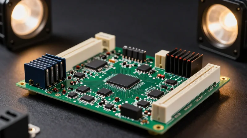
The VFD Design Environment: Balancing Power and Precision
Precision VFD PCB design is inherently difficult because it forces high-voltage power switching circuitry to coexist with sensitive, low-voltage control signals. Designers must reconcile the requirement for high-speed PWM signal integrity with the aggressive physics of power electronics, where transient voltage spikes and high-frequency noise can compromise system stability. Achieving robustness in this landscape requires moving beyond generic DFM (Design for Manufacturing) to specialized rules that prioritize clearance, creepage, and electromagnetic interference (EMI) containment.
Key Design Challenges in High-Voltage VFD Systems
| Challenge Factor | Primary Design Impact | Mitigation Strategy |
|---|---|---|
| Transient Voltage Spikes | Potential for dielectric breakdown | Increased clearance and snubber circuits |
| Thermal Density | Component degradation and drift | Strategic copper pouring and thermal vias |
| High dV/dt Switching | Coupled noise in control loops | Differential signaling and guard traces |
Compliance and Reliability Framework
Strict adherence to safety standards such as IPC-2221 and IEC 61800-5-1 is non-negotiable for VFDs. These standards define the necessary air gaps and surface paths that prevent catastrophic arcing in industrial environments. Beyond regulatory compliance, managing the board-level thermal profile is vital to prevent thermal runaway in the power stage, which can shift component tolerances and degrade overall signal precision.
- How do transient voltages impact board spacing?
Transient pulses caused by inductive kickback and fast switching transients often exceed the nominal DC bus voltage, requiring engineers to calculate clearance based on peak transient conditions rather than steady-state operating voltage to prevent arc-over. - Why is thermal stability crucial for precision VFDs?
Precision control hinges on accurate sensing; excessive heat near current sense amplifiers or reference voltage sources introduces thermal drift, leading to non-linearities and inaccurate motor control feedback. - What is the primary role of creepage distance in VFD design?
Creepage distance prevents long-term insulation failure caused by conductive path formation on the PCB surface due to humidity, pollution, or microscopic debris, ensuring long-term field reliability.
Strategic Trace Routing for Power and Signal Integrity
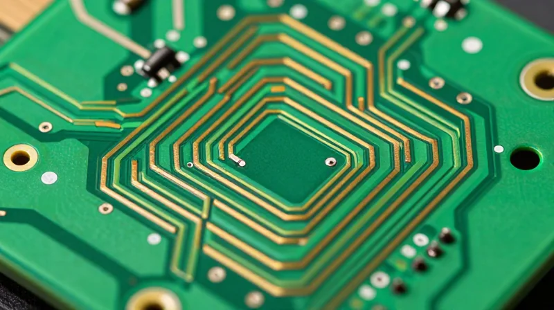
Minimizing Parasitic Inductance in Gate Drive Loops
Parasitic inductance in gate drive circuits can cause catastrophic ringing and erratic switching behavior in VFDs. To minimize this, designers must prioritize loop area reduction by keeping the gate and source/emitter traces tightly coupled, preferably utilizing a dedicated return path directly beneath the gate signal on the adjacent PCB layer.
Trace Spacing for High-Voltage Isolation
Preventing arc-over requires strict adherence to creepage and clearance standards based on your specific voltage profile and environmental contamination levels. The following table highlights standard considerations for spacing between high-voltage nodes.
| Parameter | Design Strategy | Goal |
|---|---|---|
| Clearance | Air gap between conductive paths | Prevent dielectric breakdown |
| Creepage | Surface path along insulation | Prevent tracking/carbonization |
| Conformal Coating | Dielectric barrier application | Reduce required spacing |
Design Best Practices FAQ
- How does trace width affect thermal stability?
Increased trace width lowers DC resistance, reducing I²R heat dissipation. However, for high-frequency switching lines, keep widths optimized to maintain impedance control rather than solely for current capacity. - What is the role of slots in PCB routing?
Milling slots between high-voltage pads increases the creepage distance without requiring larger board dimensions, effectively mitigating the risk of conductive path formation due to dust or humidity. - Should I use solid copper planes for high-speed signals?
Avoid large planes near high-dI/dt loops to prevent eddy current generation, which can induce noise in sensitive feedback circuits; instead, use localized, high-frequency bypass capacitor stitching.
Advanced Ground Plane Architectures

Advanced Ground Plane Architectures for VFD Reliability
In precision Variable Frequency Drive (VFD) applications, the primary goal of ground plane architecture is to suppress common-mode noise and prevent high-frequency transients from infiltrating sensitive logic circuits. Implementing a rigorous split or star grounding strategy is essential to manage the return path currents generated by rapid PWM switching in the inverter stage.
Grounding Strategy Comparison
| Strategy | Best Use Case | Key Advantage |
|---|---|---|
| Star Grounding | Low-frequency, high-precision control circuits | Eliminates common-mode loops |
| Split Planes | Isolated power and signal domains | Prevents noise injection via shared paths |
| Integrated Plane | High-density designs with fast rise times | Minimizes loop area and parasitic inductance |
Technical Implementation FAQs
- When should you implement a split ground plane?
Split planes are recommended when you must physically separate noisy DC-link capacitors or IGBT gate drive returns from the analog sensing circuits to prevent conductive coupling. - How do you manage high-frequency currents in a split system?
If you split the ground, ensure you provide a controlled low-impedance return path using a bridge component or specific connector placement, otherwise you risk creating massive EMI antennas. - What is the danger of using a single solid ground plane in VFDs?
While solid planes offer the best thermal conductivity, they allow noisy return currents to flow directly underneath sensitive traces, leading to potential ground bounce and signal degradation.
For VFD designs, the design rule is simple: maintain physical separation between high-voltage switching nodes and low-voltage control circuits. If you utilize a multi-layer stackup, dedicate an internal layer as a reference plane for control signals while keeping power-stage returns isolated on a separate dedicated plane to maintain galvanic and electromagnetic isolation.
EMI Mitigation and Electromagnetic Compatibility (EMC)
Minimizing Electromagnetic Interference through Loop Control
The primary source of radiated EMI in Variable Frequency Drives is the high-frequency current loop formed by the DC bus capacitors, power switches (IGBTs/MOSFETs), and the load return path. Reducing the physical area of these loops is the most effective defense against magnetic field coupling. Designers must prioritize the placement of decoupling capacitors as close as possible to the power semiconductor terminals to minimize the commutation loop inductance, which otherwise leads to severe voltage ringing and EMI spikes.
Effective Shielding and Partitioning Strategies
Beyond loop minimization, physical separation and shielding are critical for isolation of sensitive control signals from high-voltage switching noise. Utilize dedicated EMC shielding techniques to contain near-field emissions.
| Shielding Strategy | Implementation | Primary Benefit |
|---|---|---|
| PCB Guard Rings | Surround noisy circuits with grounded copper | Prevents noise coupling into traces |
| Faraday Cages | Metal enclosures or via-fencing | Attenuates radiated field escape |
| Differential Pairs | Tightly coupled signal routing | Improves common-mode noise rejection |
Frequently Asked Questions on EMC Compliance
- How do via-fences help in VFD EMC design?
Via-fences act as a vertical barrier that prevents electromagnetic wave propagation between internal board layers and can significantly reduce edge-radiation emissions from the PCB periphery. - What is the role of the chassis ground connection?
The chassis ground must provide a low-impedance path for high-frequency return currents to prevent the PCB from acting as an antenna, which is vital for passing CISPR 11 radiated emission tests. - Why is filter component placement critical?
EMI filters must be placed at the point of entry/exit to block conducted emissions. Placing these components too far from board connectors allows noise to couple onto cables, rendering the filtering ineffective.
Optimizing Thermal Dissipation and Heat Sink Integration
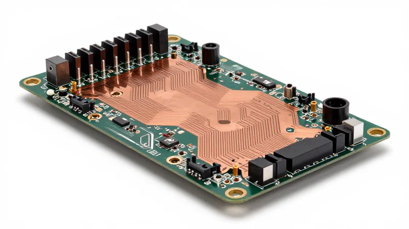
Managing High-Power IGBT Thermal Loads
Precision Variable Frequency Drives (VFDs) rely on high-switching-frequency IGBTs, which create significant localized heat flux that can jeopardize component longevity and signal integrity. To mitigate thermal runaway, designers must maximize the thermal conductivity of the PCB substrate by leveraging large-area copper pours and dense via arrays that facilitate a low-resistance path to the underlying heat sink assembly.
Thermal Via Optimization Strategy
Thermal vias serve as the vertical heat bridges between the PCB surface and the internal/bottom copper layers. For optimal thermal performance, utilize a 'stitching' pattern with the following guidelines:
- Via Pitch and Diameter
Keep thermal via pitch within 0.8mm to 1.2mm for balanced thermal transfer; drill diameters should be optimized between 0.2mm and 0.3mm to ensure effective plating during manufacturing. - Plating Thickness
Specify a minimum finished copper plating of 25um (1 mil) within the via barrels to reduce thermal resistance. - Copper Flooding
Ensure all thermal vias are tied to internal ground or power planes to increase the effective thermal mass of the board.
Comparison of Thermal Integration Techniques
| Method | Primary Benefit | Implementation Complexity |
|---|---|---|
| Copper Pour/Planes | Increased Surface Area | Low |
| Thermal Via Arrays | Z-Axis Thermal Transfer | Medium |
| Direct Heat Sink Clamping | Active/Passive Dissipation | High |
Mechanical Integration and Mounting
Mechanical mounting of heat sinks must account for the mechanical stress imparted on the PCB during thermal cycling. Use thermal interface materials (TIM) with high dielectric strength and low thermal impedance. Always prioritize rigid standoff placements near high-current components to prevent warping, which can introduce microscopic air gaps between the component body and the heat sink surface.
DFM Protocols for Component Placement

Strategic Partitioning of High-Voltage and Low-Voltage Zones
To achieve high reliability, components must be physically partitioned based on their functional voltage domains. The primary DFM rule is to establish a clear boundary between the high-power inverter stage and the low-voltage control circuitry. By enforcing a physical clearance zone that respects creepage and clearance requirements according to standards like IEC 61800-5-1, you reduce the risk of arc-over and electromagnetic interference.
Placement Priority Matrix
| Component Category | Placement Constraint | Reasoning |
|---|---|---|
| IGBT Modules | Edge/High-Thermal Zone | Maximizes airflow and simplifies heat sink mounting. |
| Gate Drivers | Proximal to IGBTs | Minimizes parasitic inductance in the gate drive loop. |
| Sensitive Logic/MCU | Far-field/Isolated Region | Ensures immunity from PWM switching noise and EMI. |
| DC Link Capacitors | Adjacent to Power Stage | Reduces ESR/ESL impact on bus voltage stability. |
Advanced DFM Guidelines for Placement
- Component Orientation
Align all polarized components in the same orientation where possible to streamline the AOI (Automated Optical Inspection) process and reduce errors during pick-and-place. - Test Point Accessibility
Ensure test points are placed on the bottom layer or accessible regions to allow for In-Circuit Testing (ICT) without needing to de-energize the entire high-voltage bus. - Solder Mask Bridges
Maintain sufficient distance between high-voltage pads to allow for solder mask dams, which prevents solder bridging during reflow of power semiconductors.
Common Placement Pitfalls
- Does component height affect thermal performance?
Yes; tall components placed upstream of heat-generating IGBTs can obstruct forced-air cooling paths, leading to localized hotspots. - How does PCB thickness influence component mounting?
For heavier VFD components, a thicker PCB (e.g., 2.4mm or higher) is recommended to prevent board bowing during reflow and to provide structural integrity for heat sink mounting.
Verification and Testing: Bridging Design to Reality
Post-Layout Verification and Prototype Validation
Transitioning from CAD files to a production-ready VFD board requires a systematic verification workflow that validates signal integrity (SI) and thermal distribution before full-scale manufacturing. By utilizing pre-production simulation alongside physical bench testing, designers can isolate potential failure points caused by parasitic inductances or inadequate thermal pathways.
| Validation Step | Primary Objective | Key Equipment |
|---|---|---|
| Transient Voltage Analysis | Verify snubbers/clamping circuits | High-bandwidth Oscilloscope |
| Thermal Imaging | Identify hot spots at load | Infrared Thermal Camera |
| TDR Reflectometry | Measure impedance continuity | Time-Domain Reflectometer |
Critical Testing Protocols for VFD Stability
- How is transient voltage stress managed during testing?
Perform double-pulse testing on the IGBT gate drive stages to evaluate turn-off voltage spikes; ensure these stay well below the component breakdown voltage under worst-case PWM switching scenarios. - What role does thermal imaging play in DFM?
Thermal imaging must be performed under sustained maximum load to detect heat accumulation in high-frequency switching regions, ensuring that thermal vias and copper pours are effectively shunting heat away from sensitive control ICs. - How can one verify isolation barrier integrity?
High-pot testing is mandatory to ensure that creepage and clearance distances defined during the DFM phase hold up under environmental humidity and pollution levels typical of industrial VFD environments.
Automated Design Rule Check (DRC) Automation
Modern VFD design demands more than basic DRC; it requires a programmatic approach to validation. Integrating custom scripts into the ECAD environment ensures that critical constraints—such as clearance around high-voltage nodes and minimum thermal relief spacing—are verified automatically.
import pcb_checker.verify as v

# Run custom constraint check for VFD isolation
result = v.check_high_voltage_creepage(min_distance=8.0)
if not result.passed:
    print(f'Critical Isolation Failure: {result.error_nodes}')
By strictly adhering to these advanced DFM rules, you can dramatically improve the reliability, thermal efficiency, and EMC compliance of your VFD hardware. Don't let layout bottlenecks compromise your industrial product lifecycle. Need help optimizing your current PCB layout for high-voltage applications? Contact our engineering team today for a comprehensive design review.
