
In the rapidly evolving world of WiFi 6 and 7, the motherboard is no longer just a passive carrier; it is a complex radio frequency environment. As clock speeds push into the multi-gigabit range, even the slightest design oversight can lead to signal attenuation, EMI failures, and non-compliance with rigorous FCC and IEEE standards. This guide provides the authoritative blueprint for balancing DFM manufacturability with the uncompromising physics of high-frequency signal integrity.
The Physics of High-Frequency Design

Beyond DC Circuitry: The Reality of High-Frequency Wave Propagation
At WiFi 6 and 7 frequencies, extending into the 6GHz and 7.125GHz bands, PCB traces can no longer be viewed simply as perfect conductors connecting nodes. Instead, they must be treated as transmission lines where signal energy propagates as electromagnetic waves through the dielectric material. As frequencies increase, the wavelength shortens, causing parasitic capacitance and inductance—previously negligible at low speeds—to dominate signal behavior. Engineers must account for the skin effect, dielectric loss, and electromagnetic interference (EMI) that can catastrophically degrade the SNR required for high-order modulations like 4096-QAM.
Traditional vs. Advanced Design Paradigms
| Parameter | Legacy Design (DC/Low-Speed) | WiFi 6/7 Design (6GHz+) |
|---|---|---|
| Signal Analysis | Ohm's Law / KVL/KCL | Maxwell's Equations / S-Parameters |
| Trace Modeling | Ideal Conductor | Controlled Impedance Transmission Line |
| Via Geometry | Geometric Connection | Inductive Discontinuity / Impedance Mismatch |
| Skin Effect | Ignored | Dominant factor in signal attenuation |
Frequently Asked Questions on RF Physics
- Why does impedance control become critical at 6GHz?
At high frequencies, any deviation from the target impedance (typically 50 ohms) causes signal reflections, leading to standing waves and massive insertion loss that disrupts the tight timing margins of OFDM signals. - How does the skin effect impact motherboard fabrication?
The skin effect forces current to flow near the surface of the copper trace. This increases effective resistance and necessitates the use of smoother copper foil to prevent signal degradation caused by roughness-induced losses. - What role does dielectric constant (Dk) stability play?
Variations in Dk across the board surface cause phase velocity changes, leading to timing skews. WiFi 7 demands tight Dk tolerance to maintain coherent phase relationships across multi-input multi-output (MIMO) antenna arrays.
Achieving Precise Impedance Control
The Geometry of Impedance Stability
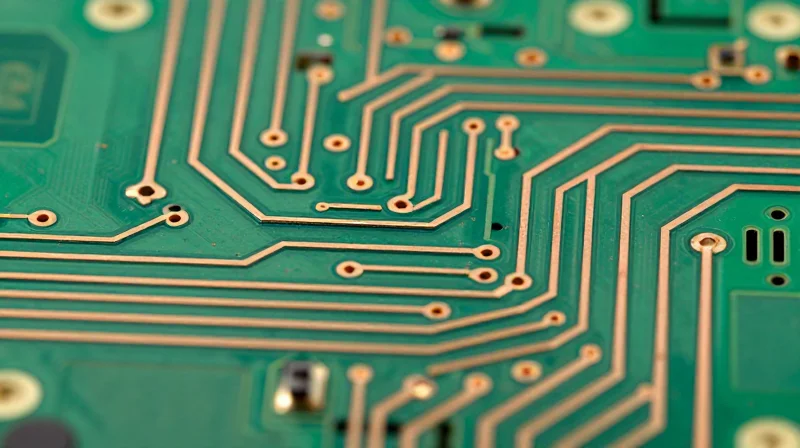
Maintaining target 50-ohm single-ended or 100-ohm differential impedance at frequencies exceeding 6GHz demands more than simple calculator outputs. Designers must account for the etch factor, which significantly alters track geometry during fabrication. A trapezoidal trace shape—inherent to subtractive PCB manufacturing—means the width at the base differs from the top, directly impacting the capacitive coupling and resulting impedance. For WiFi 7 applications, selecting high-frequency, low-loss laminates (such as Megtron 6 or 7) with a stable dielectric constant (Dk) across the frequency sweep is non-negotiable.
| Parameter | WiFi 6 (6GHz) | WiFi 7 (7.125GHz+) | Impact on Impedance |
|---|---|---|---|
| Dk Tolerance | ±0.05 | ±0.02 | High |
| Surface Roughness | Standard VLP | HVLP/Hyper-Low | Significant |
| Etch Compensation | Standard | Advanced | Medium |
Critical DFM Strategies for Differential Pairs
- How does glass weave affect high-speed signals?
The heterogeneous nature of fiberglass (glass bundles vs. resin) creates Dk variations. For WiFi 7, utilize 'spread glass' styles like 1067 or 1078 to ensure signals experience a uniform dielectric environment, preventing skew and impedance discontinuities. - Why is copper roughness a priority for WiFi 7?
At high frequencies, the skin effect forces current to flow near the conductor surface. High-profile copper roughness increases insertion loss and causes localized impedance variance, degrading signal integrity. Specify Hyper-Low Profile (HVLP) copper foils. - What is the role of reference plane continuity?
Any split in the reference plane beneath a high-speed trace creates a loop area, resulting in an impedance spike. Ensure solid, continuous ground planes directly beneath all WiFi signal paths to maintain a constant return path.
Advanced Stack-up Optimization
To guarantee 100-ohm differential impedance, focus on the 'stripline' configuration rather than 'microstrip' where possible. Stripline provides inherent shielding and reduced radiation, which is critical for meeting stringent FCC/ETSI electromagnetic compatibility requirements at WiFi 7 frequencies. Always request a TDR (Time Domain Reflectometry) coupon from the manufacturer to verify that the manufactured impedance matches the design intent within a ±5% tolerance band.
Crosstalk Mitigation Techniques
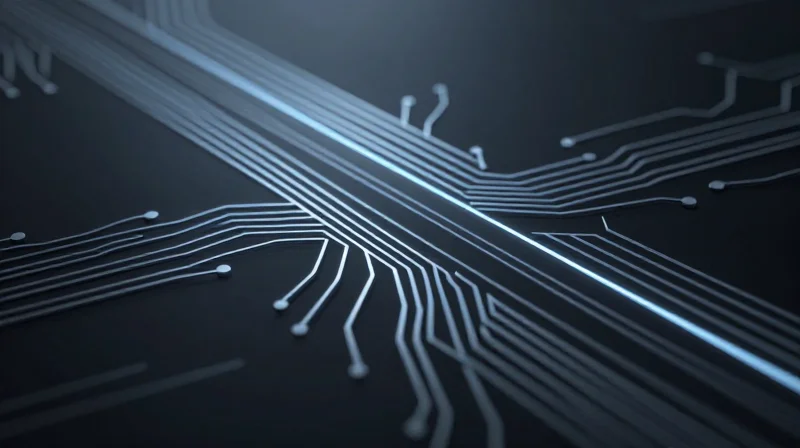
At WiFi 6E and WiFi 7 frequencies (up to 7.125GHz and beyond), electromagnetic coupling between adjacent traces becomes a primary failure vector. Crosstalk is not merely an inconvenience; it manifests as jitter, bit-error-rate (BER) degradation, and massive throughput loss. Mitigating these effects requires moving beyond standard DRC rules toward field-solver-driven constraints and rigorous geometric isolation.
Advanced Isolation Strategies
- The 3H Rule and Beyond
While the 3H rule (where separation is three times the trace height above the plane) is a baseline, WiFi 7 demands a 5H minimum distance in high-speed digital regions to minimize mutual capacitance and inductance. - Guard Trace Utility
Guard traces are effective only when properly grounded via stitching vias at intervals less than 1/10th of the wavelength of the highest signal frequency, ensuring the guard acts as a true reference sink rather than a resonator. - Via Fence Architecture
Utilize via fences along the periphery of high-speed RF traces to contain edge-fire radiation, particularly when routing near sensitive analog front-end (AFE) circuitry.
Comparative Analysis of Coupling Suppression
| Technique | Coupling Reduction | Implementation Complexity | Best Use Case |
|---|---|---|---|
| Increased Spacing | High (Exponential) | Low | General board routing |
| Differential Shielding | Medium | Medium | High-speed bus routing |
| Grounded Guard Traces | Very High | High | Isolation of RF paths |
| Layer Stripline Isolation | Extreme | High | Layer transitions |
Layer Assignment Best Practices
To fundamentally eliminate crosstalk, layer assignment must prioritize orthogonal routing. By alternating signal layers between horizontal (X) and vertical (Y) orientations, the parasitic overlap area between parallel traces is minimized. Furthermore, maintain the 'Signal-GND-Signal' sandwich structure to ensure that every high-speed trace has an immediate, low-impedance return path, significantly reducing the loop area that contributes to inductive coupling.
Design Rule Verification
/* Example Field Solver Constraint Syntax */
CONSTRAINT_SET_NAME: WIFI_7_RF_ISOLATION
MAX_PARALLEL_RUN: 5.0mm
MIN_ISOLATION_DISTANCE: 0.25mm
VIA_STITCHING_INTERVAL: 1.0mm
REFERENCE_PLANE: GND_LAYER_2
IMPEDANCE_TOLERANCE: +/- 5%
Optimizing Via Stitching for EMI Reduction
The Role of Via Fencing in EMI Containment
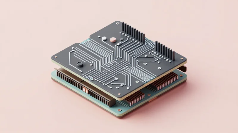
At WiFi 7 frequencies, signals behave as waves rather than simple currents. Via fencing creates a Faraday cage effect around high-speed differential pairs, preventing electromagnetic field leakage into the PCB substrate. By placing stitching vias at intervals strictly less than one-tenth of the wavelength ($λ/10$) of the highest harmonic, designers can effectively trap noise and suppress resonance modes.
Design Guidelines for Optimal Stitching
| Parameter | Recommended Practice | Impact |
|---|---|---|
| Via Pitch | <λ/20 at max freq | Prevents slot antenna formation |
| Stitch Proximity | 2x to 3x dielectric thickness | Minimizes loop inductance |
| Return Path Vias | Placed at layer transitions | Maintains reference continuity |
Common Implementation Challenges
- How does stitching density impact board manufacturing?
Increased stitching density adds drilling time and potential for layer misalignment; ensure your CM validates the drill-to-copper clearances for high-density stitching patterns. - Why is 'via stitching' vital for layer transitions?
When a signal travels between layers via a via, the return current must also transition; placing a ground stitch via immediately adjacent to the signal via ensures the return current loop remains minimized. - Does over-stitching cause issues?
Excessive stitching can lead to 'moating' or excessive copper removal in internal planes, which compromises power integrity and thermal dissipation; always simulate to find the balance.
Advanced Mitigation Logic
For WiFi 6/7 specifically, focus on stitch via placement at the RF front-end module (FEM) periphery. Utilizing a 'stitching perimeter' around the RF section acts as a shield against digital noise injected by the SoC or memory interfaces. Ensure that these vias are tied to the primary ground plane to minimize impedance discontinuities at the transition zones.
Dielectric Selection and Skin Effect
Dielectric Selection for Ultra-High Frequencies
At WiFi 6E and 7 frequencies, standard FR-4 substrates suffer from excessive dielectric absorption and signal attenuation. Designers must pivot to ultra-low loss (ULL) laminates to keep insertion loss within acceptable margins. Materials such as Panasonic Megtron 6 or similar high-Tg, low-Dk/Df variants are mandatory for RF signal paths to ensure minimal energy dissipation across long transmission lines.
| Material Class | Dielectric Constant (Dk) | Dissipation Factor (Df) | Primary Application |
|---|---|---|---|
| Standard FR-4 | 4.4 - 4.8 | 0.020 | Low-speed logic |
| Mid-Loss Laminate | 3.8 - 4.0 | 0.008 | PCIe Gen 3/4 |
| Megtron 6 / ULL | 3.4 - 3.6 | 0.002 | WiFi 6/7, 10G+ Ethernet |
Addressing the Skin Effect
The skin effect becomes a dominant factor at frequencies above 5GHz, where current density crowds toward the outer surface of the copper conductor, effectively increasing AC resistance. To combat this, trace geometry must be optimized beyond simple width and spacing calculations.
- Why does copper foil roughness matter?
Increased surface roughness increases the effective path length for high-frequency electrons, exacerbating skin effect losses. Using VLP (Very Low Profile) or HVLP (Hyper Very Low Profile) copper foil is essential for minimizing these parasitic resistive losses. - How does trace geometry impact performance?
Widening traces reduces DC resistance but increases capacitance; therefore, balancing trace width with dielectric thickness is required to maintain the target impedance while minimizing the surface area-to-volume ratio issues caused by the skin effect.
DFM Best Practices for RF Performance
Designers should maintain a strictly controlled reference plane directly beneath RF transmission lines. Avoid crossing splits or gaps in the reference plane, as the return current paths at high frequencies will follow the path of least inductance—directly under the signal—rather than the path of least resistance.
Navigating FCC and IEEE Compliance
Navigating FCC and IEEE Compliance
Achieving FCC Part 15 and IEEE 802.11ax/be compliance for WiFi 6/7 motherboards requires a proactive design-for-compliance (DFC) strategy that treats spectral purity as a primary constraint rather than a post-layout afterthought. Because WiFi 6 and 7 operate at higher modulation rates and utilize wider channel bandwidths (up to 320 MHz), even minor impedance mismatches or poor return paths can lead to non-compliant spurious emissions, forcing costly board respins.
Regulatory Compliance Checklist
- Spectral Mask Adherence
Ensure all layout designs maintain strict out-of-band rejection. Use high-Q bandpass filters specifically tuned for the 6GHz U-NII-5 through U-NII-8 bands to avoid IEEE spectral density violations. - Radiated Emission Control
Minimize unintentional radiator effects by utilizing a 20H rule for power planes, ensuring that ground planes extend beyond the power planes to prevent edge-radiation. - Via Fence Density
For high-frequency RF traces, maintain via stitching spacing at 1/10th or 1/20th of the wavelength (λ) of the highest operating frequency to prevent slot antenna effects.
| Requirement Type | Regulatory Target | DFM Focus Area |
|---|---|---|
| FCC Part 15 | Spurious Emissions | Shielding & Via Fences |
| IEEE 802.11be | EVM & Phase Noise | Impedance & Loss Control |
| EU RED (ETSI) | Dynamic Frequency Selection | Trace Length Matching |
To ensure long-term regulatory approval, designers must focus on the interface between the RF front-end and the baseband processor. The trace transitions must be modeled as discrete discontinuities. Using 3D EM simulation, verify that the return loss ($S_{11}$) remains below -15dB at the 7.125 GHz upper limit. Neglecting these high-frequency nuances often results in failure during radiated emission testing due to harmonic generation from the clock distribution networks.
DFM: Bridging the Gap Between Prototype and Mass Production
Transitioning from Prototype to Production
The gap between a functional WiFi 6/7 prototype and a mass-produced motherboard is bridged by rigorous Design for Manufacturing (DFM) protocols. While a prototype focuses on verifying signal integrity and spectral compliance, production-ready designs must prioritize manufacturing tolerances, assembly speed, and material utilization to ensure consistent high-frequency performance at scale.
| Parameter | Prototype Focus | Mass Production Focus |
|---|---|---|
| Material Selection | Highest possible performance | Cost vs. Performance optimization |
| Tolerance Control | Individual board tuning | Statistical process control |
| Via Integrity | Manual via placement | Automated drilling/plating yields |
Key DFM Considerations for High-Yield Assembly
- Copper Balancing
Asymmetrical copper distribution leads to board warpage during the reflow process. Implement balanced copper fill patterns across all signal layers to ensure thermal uniformity during lamination and assembly. - Drill-to-Copper Clearances
Increase drill-to-copper clearances for high-density WiFi 7 layers to account for drill wander and thermal expansion, preventing internal shorts that are difficult to diagnose in post-production testing. - Manufacturing Tolerances
Specify tighter impedance tolerances at the design stage. Work with manufacturers to ensure the etching process can support the narrow linewidths required for 6GHz+ WiFi 7 bands without violating width-to-spacing ratios.
Optimizing for Automated Assembly
To minimize assembly issues, engineers must standardize fiducial placement and panelization. For high-frequency WiFi modules, ensure the panel layout minimizes mechanical stress during depanelization, as vibrations can create microscopic fractures in high-frequency signal traces or impact the impedance profile of critical transmission lines.
# Example DFM Checklist for WiFi 7 Layers
check_drill_alignment: True
verify_copper_density: '> 30% per layer'
check_impedance_tolerance: '±5%'
validate_via_stitching_clearance: 'minimum 3x dielectric height'
Verification and Simulation Protocols

The Necessity of Pre-Layout EM Simulation
Pre-layout electromagnetic (EM) simulation serves as the foundational gatekeeper in WiFi 6/7 PCB development. By analyzing stack-up geometry, trace widths, and via transitions before a single net is routed, designers can identify potential resonances and impedance discontinuities that are impossible to fix once the board is fabricated. Utilizing 2D and 3D field solvers allows engineers to characterize high-frequency dielectric behavior and confirm that impedance targets are met across the 6GHz+ spectrum.
Post-Layout Signal Integrity Analysis
Once routing is complete, post-layout analysis shifts the focus to physical reality. This phase involves extracting parasitic data from the finalized layout to assess crosstalk, reflection, and jitter. In WiFi 7 environments, even minor coupling between the high-speed data lines and RF front-end circuitry can cause massive performance degradation. Advanced SI tools must perform frequency-domain analysis up to the third or fifth harmonic of the carrier frequency to ensure signal mask compliance.
| Analysis Type | Primary Metric | Key Objective |
|---|---|---|
| Pre-Layout | Impedance & Insertion Loss | Constraint setup and material selection |
| Post-Layout | Eye Diagram & ISI | Timing closure and EMI mitigation |
Frequently Asked Questions
- Why is 3D EM simulation required for WiFi 7?
WiFi 7 utilizes wide channels and complex modulation like 4096-QAM, making it extremely sensitive to small impedance mismatches and via stubs that 2D analysis cannot accurately model. - How does via stitching affect simulation complexity?
Extensive via stitching creates dense ground return paths; while it reduces EMI, it significantly increases computational load during simulation, requiring targeted sub-circuit analysis.
Successfully deploying WiFi 6/7 hardware requires a harmonious integration of mechanical DFM and electromagnetic theory. By mastering controlled impedance, via stitching, and material choice, your team can accelerate time-to-market while ensuring robust, complaint performance. Contact our engineering consultants today to audit your current PCB designs and ensure your infrastructure is ready for the multi-gigabit era.
