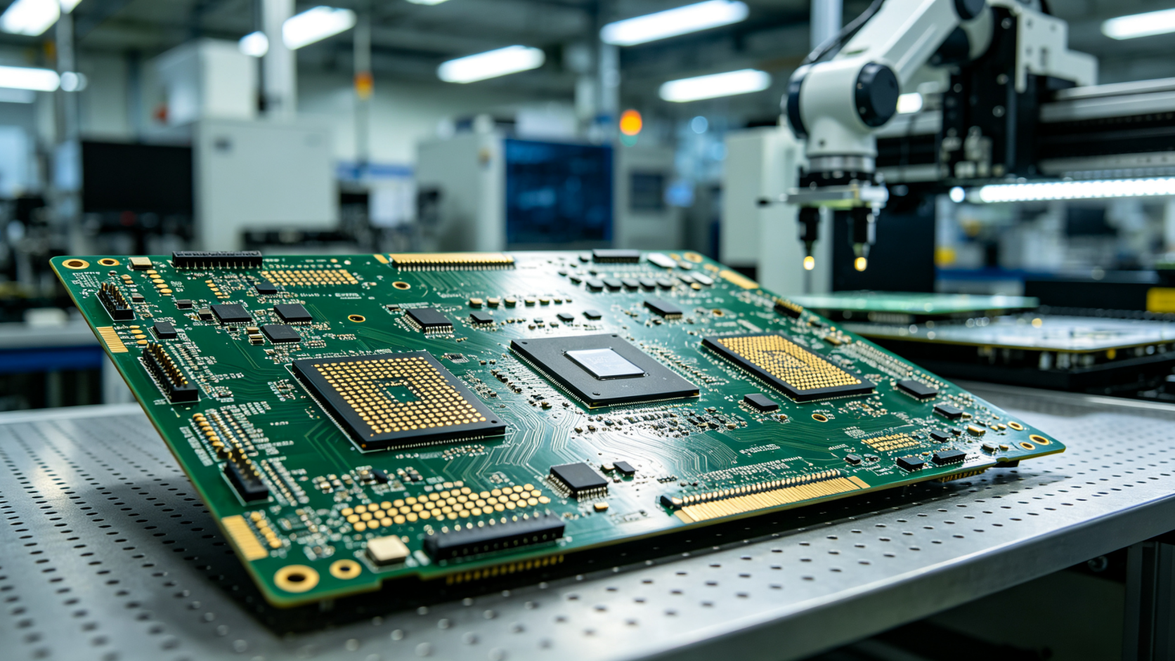
AI servers are fundamentally different from general-purpose computing servers. The difference is not just in the number of GPUs — it's in the workload characteristics that have fundamentally changed PCB design priorities and manufacturing limits.
Based on experience with multiple AI accelerator cards and NVMe switch backplane projects, AI servers push PCBs to new extremes across four dimensions simultaneously: power density, signal speed, thermal cycling life, and impedance consistency.
This guide breaks down the 5 critical specifications that define AI server PCBs — and what hardware engineers need to know to design for manufacturability.
The Challenge:
AI accelerators like NVIDIA H100 or AMD MI300X consume 700-800W peak power per GPU, delivered through 48V or 12V power distribution networks on the PCB. This means power plane copper must handle DC currents exceeding 200A.
Standard FR-4 with 1oz (35μm) copper cannot meet this requirement. AI server PCBs typically require 2oz or even 3oz heavy copper designs, with multiple parallel power planes to reduce DC voltage drop.
| Copper Weight | Thickness | Typical Application |
|---|---|---|
| 1oz | 35μm | Standard boards |
| 2oz | 70μm | AI servers, high-power |
| 3oz | 105μm | Extreme power designs |
Design Recommendations:
Via current capacity: A single 0.3mm via can carry approximately 2-3A. A 200A load requires at least 70 parallel vias, distributed evenly to balance heating.
Uneven via distribution creates localized hot spots that can cause copper blistering or dielectric carbonization.
Power plane design: Use multiple parallel power planes to reduce DC resistance and improve current distribution.
Thermal management: Perform electro-thermal co-simulation to identify hot spots before layout.
The Challenge:
In AI training clusters, interconnects between GPUs, between GPU and HBM memory, and between GPU and NVSwitch have fully entered the 56Gbps NRZ and 112Gbps PAM4 era. At these speeds, PCB insertion loss becomes the critical variable determining link budget.
Total insertion loss per inch (dielectric loss + conductor loss) must be controlled within 0.5dB. This imposes苛刻 requirements on the material's dissipation factor (Df).
| Material Type | Df (Dissipation Factor) | Application |
|---|---|---|
| Standard FR-4 | ~0.02 | General purpose |
| Mid-loss materials | ~0.010-0.015 | 10-25G designs |
| Ultra-low-loss materials (M7N, MW4000) | 0.004-0.006 | AI servers, 112G |
Design Recommendations:
Material selection: AI servers require ultra-low-loss materials like M7N or MW4000 series, with Df between 0.004-0.006.
Dk stability: Ensure dielectric constant drift is less than ±2% across -40°C to 105°C.
Loss verification: Test data shows that on equivalent 10-inch differential pairs, ultra-low-loss materials reduce insertion loss by approximately 35% compared to mid-loss materials — directly determining whether 112G links can open valid eye diagrams.
Roughness control: Copper foil surface roughness significantly affects conductor loss at high frequencies. Specify low-profile or ultra-low-profile copper foils for high-speed layers.
The Challenge:
In AI servers, high-speed signals need to switch between different inner layers through multilayer boards. Vias inevitably create stubs. For 112G PAM4 signals, even 8-10mil of residual stub creates resonance frequencies that fall within the signal bandwidth, causing不可忽略 return loss.
The Specification:
Back-drilled residual stub length must be controlled within 4mil, with back-drill depth tolerance of ±2mil.
Design Recommendations:
Capability verification: Confirm your manufacturer's back-drill depth control capability before design.
Board thickness uniformity: Variations in thickness directly affect back-drill accuracy — specify tight tolerances.
X-ray alignment: Multi-layer registration accuracy is critical for consistent back-drill results.
Design for back-drill: Avoid routing directly above or below back-drill areas to prevent accidental damage.
Test coupon: Include back-drill test coupons on the panel edge for verification.
The Challenge:
AI servers typically run 24/7 at full load, with frequent temperature fluctuations. The CTE (Coefficient of Thermal Expansion) mismatch between GPU chips and PCB creates stress concentrated on BGA solder balls.
| Specification | Standard PCB | AI Server PCB |
|---|---|---|
| Tg (Glass Transition Temperature) | ~150°C | ≥170°C |
| CTE (Z-axis) | ~60 ppm/°C | ≤50 ppm/°C |
| Plated hole wall copper | ~20μm | ≥25μm |
Design Recommendations:
Material selection: Use high-Tg (≥170°C) materials with Z-axis CTE ≤50 ppm/°C.
Plating thickness: Specify minimum 25μm copper thickness in plated through-hole walls.
Thermal cycling testing: Verify that the design survives 500+ thermal cycles without via corner cracking.
Via protection: Consider via-in-pad with copper filling for critical BGA escape vias.
Reliability Data:
In reliability testing, standard materials showed up to 8% via crack rate after 300 thermal cycles. High-Tg materials with thick copper reduced this to below 0.5%.
The Challenge:
General-purpose servers typically specify ±10% differential impedance tolerance. AI servers tighten this to ±5% for 112G differential pairs.
| Tolerance | Application | Requirements |
|---|---|---|
| ±10% | General-purpose servers | Standard manufacturing capability |
| ±5% | AI servers | Tight process control, specialized materials |
Design Recommendations:
Line width tolerance: Must be controlled within ±0.5mil.
Dielectric thickness: Thickness variation must not exceed ±5% across the board.
Etching factor (undercut): Must be stable below 0.5mil.
3D electromagnetic simulation: Use 3D EM field simulation to calibrate impedance discontinuities at interfaces between different dielectric materials.
Material interfaces: AI accelerator cards often use mixed-layer structures with materials like Megtron 6. Each material interface requires individual calibration.
AI server PCBs typically have:
Layer count: 20-32 layers
Blind/buried vias: 3-5× more than standard servers
Dielectric thickness: Ultra-thin (3-4mil)
Fine lines: 3.5/3.5mil trace/space
These specifications result in:
Yield: 15-20% lower than standard products
Test coverage: 100% electrical test required (flying probe + TDR)
Lead time: 14-18 days (vs. 7 days standard)
Cost: 2-4× higher than standard PCBs
| Specification | AI Server Requirement | Why It Matters |
|---|---|---|
| Copper Weight | 2-3oz | 200A+ current handling |
| Insertion Loss | Less than 0.5dB/inch | 112G PAM4 signal integrity |
| Material Df | 0.004-0.006 | Ultra-low-loss laminates |
| Back-Drill Stub | Less than 4mil | 112G return loss control |
| Tg | ≥170°C | Thermal cycling reliability |
| CTE (Z-axis) | ≤50 ppm/°C | BGA solder joint integrity |
| Impedance Tolerance | ±5% | 112G signal quality |
| Layer Count | 20-32 layers | Routing density |
???? www.anypcba.com
???? We specialize in small-to-medium batch PCB and PCBA — from prototypes to production. If you're designing AI server PCBs and facing challenges with these specifications, send us your files. We'll provide a DFM review and a transparent quote.




