High-speed serial links require tight control of differential impedance, skew, and coupling to limit reflections, mode conversion, and crosstalk. At multi-gigabit data rates, small deviations in trace geometry, routing symmetry, or material properties can corrupt the eye diagram and cause protocol non-compliance.
This guide reviews the key signal integrity requirements for differential pairs in high-speed serial interfaces: differential impedance control, skew management, crosstalk reduction, and PCB layout techniques that preserve signal quality from driver to receiver.
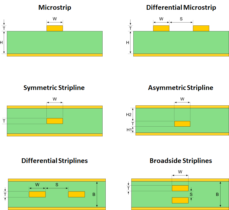
Differential impedance is the primary electrical parameter governing signal transmission on a routed differential pair. It equals twice the odd-mode impedance of each line and depends on trace width, intra-pair spacing, copper thickness, dielectric height, and dielectric constant.
Common target impedances for serial interfaces:
| Interface | Differential Impedance |
|---|---|
| PCIe Gen 4/5 | 85Ω |
| USB 3.2 / USB4 | 90Ω |
| LVDS | 100Ω |
Key Design Principles:
Controlled stackup: Maintain target impedance through a controlled stackup. Trace geometry must be correlated with field solvers or manufacturing impedance tables, with width and spacing held constant across the entire pair length.
Avoid discontinuities: Neck-downs, anti-pads, asymmetric via structures, and asymmetrical component pads introduce local impedance perturbations that generate reflections and degrade eye opening.
Component symmetry: Small passive components like AC coupling capacitors should use 0402 or smaller packages, with both legs arranged symmetrically to minimize component-induced asymmetry.
Reference plane integrity: A solid, continuous reference plane beneath or around the pair is essential. Microstrip pairs route over continuous ground planes; stripline pairs route between ground or power planes. Plane splits, voids, or gaps beneath the pair raise local impedance and increase radiated fields.
Impedance tolerance: ±10% impedance tolerance is typical and should appear in fabrication notes and be enforced in PCB tools as net-specific constraints.
Calculation tools: Closed-form equations like IPC-2141 provide approximations that lose accuracy at high frequencies. Field-solver-based tools, including calculators like Polar SI9000, provide more reliable starting geometries. For critical links, S-parameter or TDR simulation should verify achieved impedance before fabrication.
Skew is the propagation delay difference between the P and N legs of a differential pair. It converts differential energy into common-mode noise, degrading eye opening and increasing electromagnetic radiation.
Key Design Principles:
Symmetrical routing: The most common cause of skew is non-symmetrical routing. Skew occurs when the two legs of a differential pair experience unequal path lengths, corrected by distributed serpentine tuning while avoiding local discontinuities.
Geometry symmetry: Maintain geometric symmetry between the two legs — same bend count, matching structures, parallel paths over the same reference plane. This eliminates most routing-induced delay mismatches.
Distributed length tuning: When length adjustment is needed, serpentine segments on the shorter leg restore phase alignment. Distributed tuning over a longer trace segment is preferred over compact serpentines placed near connectors or receivers, which introduce local capacitive loading and crosstalk.
Via structures: Each via adds capacitive loading and, without back-drilling, leaves a stub that resonates at frequencies inversely proportional to stub length. Matching via positions on both legs, combined with back-drilling in high-speed designs, keeps skew within budget.
Glass weave effect: Standard FR-4 laminates can introduce 10-100ps of skew at 10Gbps and above. One leg may route predominantly over glass bundles, the other over resin-rich areas, creating different effective dielectric constants and propagation speeds.
Low-Dk materials: Low-Dk, low-variation laminates, slight trace angle offsets relative to weave direction, or materials with known weave skew compensation reduce this effect in demanding designs.
Complete path matching: Skew matching should account for the complete signal path — package traces, connector pins, and via delays — not just PCB trace lengths.
Differential signaling rejects common-mode noise and enhances immunity to external aggressors. However, when spacing and referencing are insufficient, parallel high-speed nets can still couple to each other and to adjacent single-ended nets.
Key Design Principles:
Tight intra-pair coupling: Close spacing between P and N legs reduces loop area and radiated fields, improving common-mode rejection.
Inter-pair spacing: The edge-to-edge spacing between adjacent differential pairs should be at least three times the dielectric height, or roughly five times the intra-pair spacing. This keeps differential crosstalk within acceptable limits for most multi-gigabit interfaces.
Reference plane proximity: Closer reference planes reduce the spacing required between pairs for a given crosstalk target — one reason stripline routing achieves better crosstalk performance than microstrip at equivalent spacing.
Physical isolation: Aggressor nets such as clock traces, DDR buses, and fast-switching power nets should not run parallel to sensitive differential channels over long distances. Coupling energy scales with parallel run length regardless of spacing.
Routing strategy: Minimizing parallel overlap and assigning sensitive pairs to layers away from noisy nets is more effective than adjusting spacing alone.
High-speed serial interfaces like PCIe Gen 4/5, USB4, and LVDS require consistent, symmetrical, and discontinuity-minimized routing.
Key Design Principles:
Straight routing: Route each pair as straight as possible with minimal layer changes. When layers must change, both legs transition together through matched vias.
Constant geometry: Maintain consistent spacing and width across the entire pair, including through bends. Shallow 45-degree bends or arc-based routing reduce impedance perturbations compared to 90-degree turns.
Component symmetry: Place AC coupling capacitors, ESD protection devices, and connector pads symmetrically on both legs with stub lengths minimized. Asymmetric component placement creates imbalance and mode conversion.
Constraint-driven routing: PCB design tools allow net-specific rules for differential impedance, intra-pair spacing, length, skew tolerance, and via usage. Defining these constraints before routing prevents manual edits or autorouting decisions from breaking symmetry.
SI simulation: For PCIe Gen 5 (32 GT/s) and USB4 (40 Gbps) designs, SI simulation using extracted S-parameters and eye diagram analysis should validate the channel before fabrication.
Mechanical considerations: Locating screws and stiffeners near connectors rather than at board corners reduces board flexing and solder joint stress during assembly and thermal cycling. Connectors near rigid attachment points experience less thermomechanical displacement — particularly important for differential connectors where contact geometry affects impedance and insertion loss.
| Requirement | Rule of Thumb |
|---|---|
| Differential Impedance | 85-100Ω (specify in fab notes, enforce as net constraint) |
| Impedance Tolerance | ±10% typical |
| Intra-pair Spacing | Maintain constant across entire pair length |
| Inter-pair Spacing | ≥3× dielectric height (or 5× intra-pair spacing) |
| Skew (Intra-pair) | ≤ few ps (depends on data rate; use distributed tuning) |
| Length Matching | Match complete signal path, not just PCB traces |
| Layer Change | Both legs transition together through matched vias |
| Component Placement | Symmetrical on both legs, stub lengths minimized |
| Reference Plane | Continuous, no splits or voids beneath pair |
| SI Validation | S-parameter + eye diagram simulation for critical links |
???? www.anypcba.com
???? We specialize in small-to-medium batch PCB and PCBA — from prototypes to production. If you're designing high-speed serial links and need help with signal integrity, send us your files. We'll provide a DFM review and a transparent quote.




