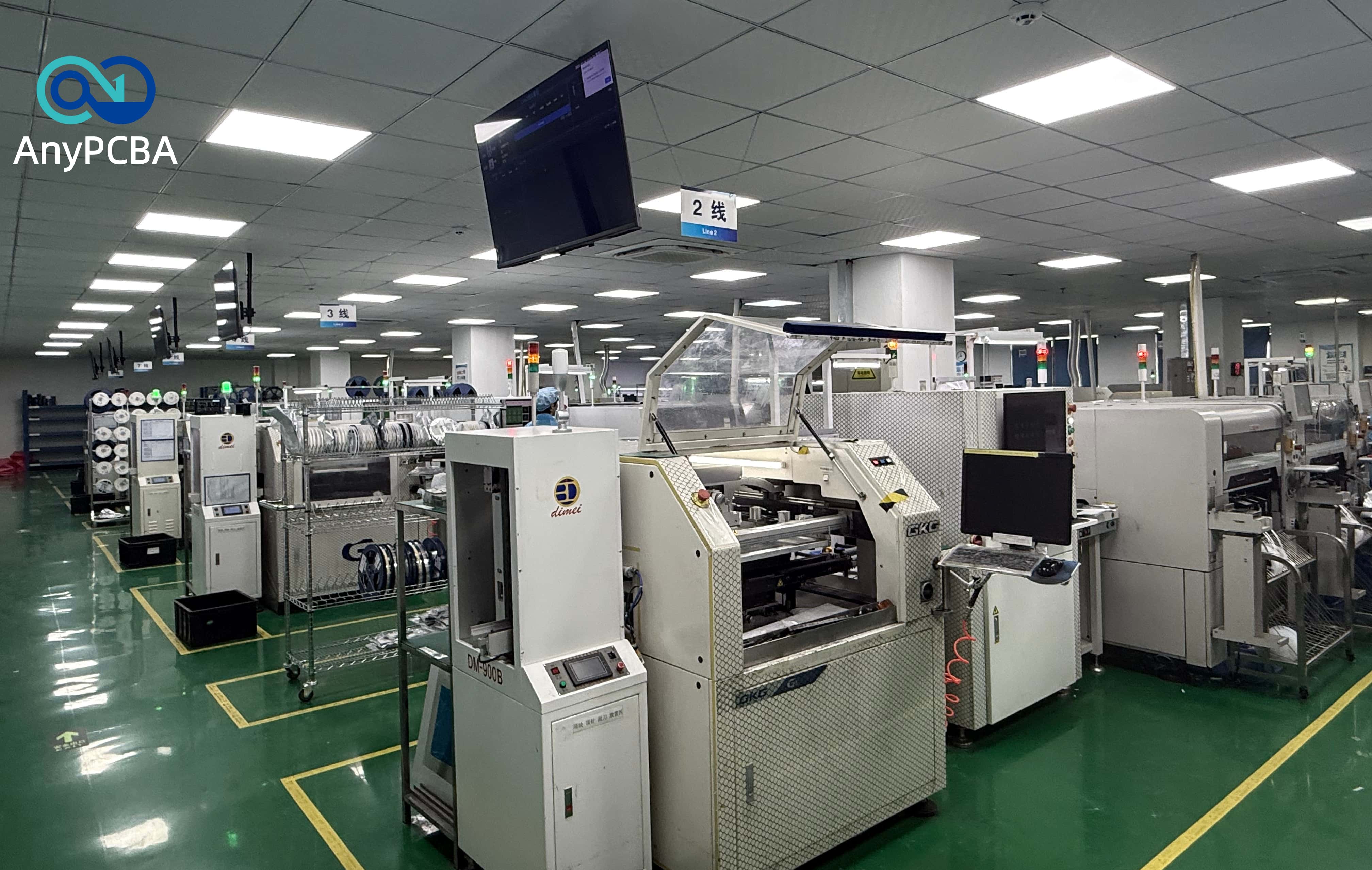
Surface mount technology (SMT) is the core process in modern PCBA manufacturing. It's the reason why today's circuit boards can pack thousands of components into a space that once held a few dozen through-hole parts.
For hardware engineers, understanding this process is not just about knowing "how boards get built." It's about making better design decisions — decisions that affect cost, yield, and lead time.
This guide covers the complete SMT assembly process — from solder paste printing to reflow soldering and inspection — with practical design recommendations for each stage.
Solder paste printing is the foundation of SMT assembly. The paste — a mixture of solder alloy powder and flux — is applied to the PCB through a stencil that matches the pad pattern.
The process:
A stencil (typically laser-cut stainless steel) is aligned over the PCB
A squeegee moves across the stencil, forcing solder paste through the apertures
The PCB separates from the stencil, leaving paste deposits on each pad
Why it matters:
| Quality Issue | Consequence |
|---|---|
| Too much paste | Bridging, solder balls |
| Too little paste | Dry joints, tombstoning |
| Misaligned printing | Open circuits |
Design Recommendations:
Stencil thickness: For fine-pitch components (0.4mm pitch QFN or 0.35mm CSP), use thinner stencils (typically 0.1-0.12mm)
Aperture design: Use trapezoidal or rounded apertures for better paste release
Nanocoating: Consider nanocoated stencils for improved release and extended cleaning cycles
Pad design: Ensure pad sizes are matched to component specifications
After paste printing, the PCB moves to the pick-and-place machine. High-speed placement machines use vacuum nozzles to pick components from feeders and place them onto the PCB with precision.
Machine types:
| Type | Application | Speed | Accuracy |
|---|---|---|---|
| High-speed mounters | Small passives (0201, 0402, 0603) | Greater than 20,000 CPH | ±50μm |
| Fine-pitch mounters | QFP, BGA, connectors | 5,000-10,000 CPH | ±25μm |
| Mixed machines | General production | 10,000-20,000 CPH | ±40μm |
Design Recommendations:
Component spacing: Leave at least 0.5mm between components for nozzle clearance
Polarity marks: Ensure polarity marks (for diodes, ICs, tantalum capacitors) are clearly visible and not covered by solder mask
Alignment targets: Include fiducial markers (1-2mm diameter) at board corners for machine alignment
Orientation consistency: For multi-pin ICs, ensure pin 1 marking is unambiguous
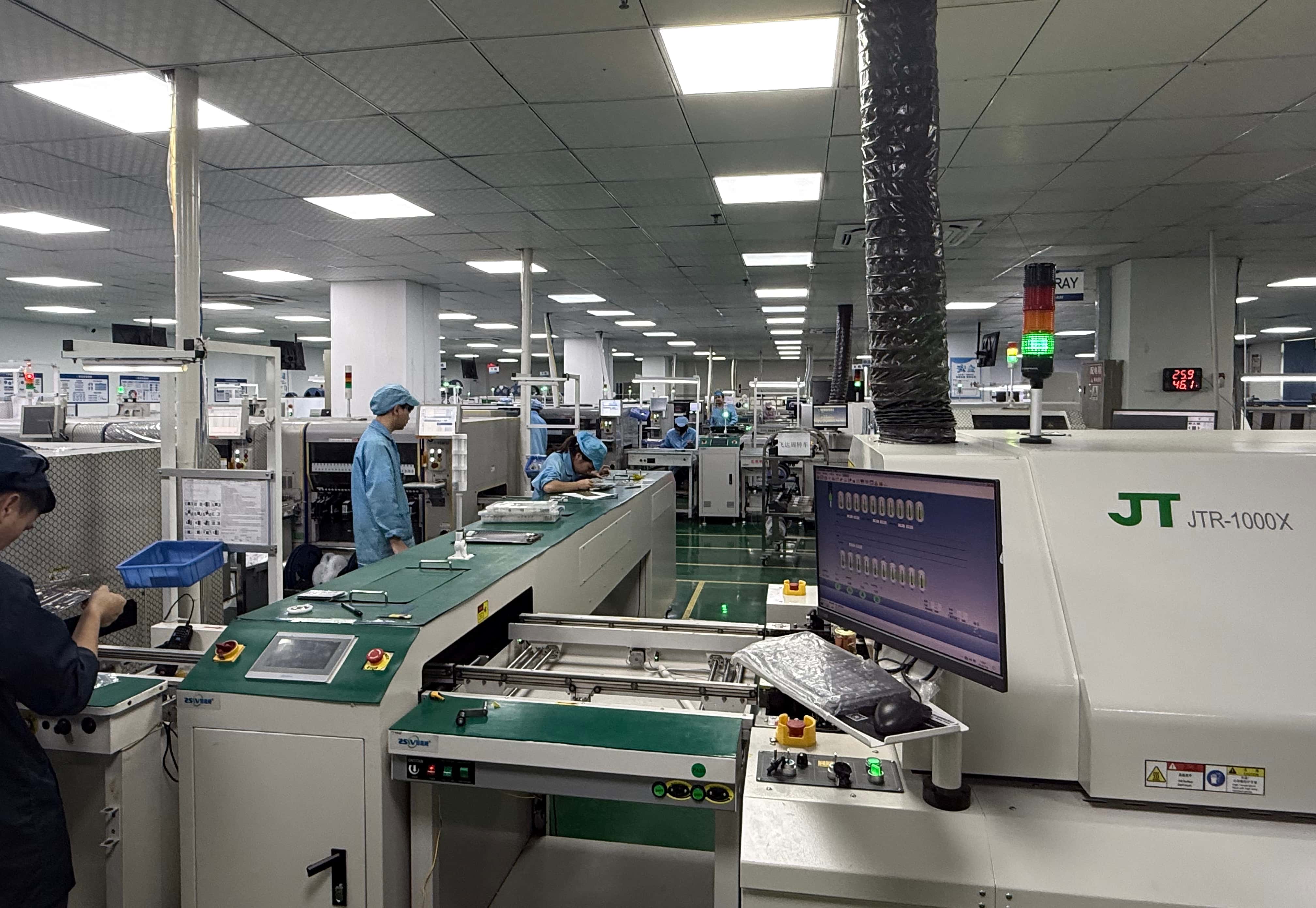
After placement, the PCB enters the reflow oven. The board is heated to melt the solder paste, which wets the pads and component leads, forming reliable solder joints.
The temperature profile:
| Zone | Temperature | Purpose |
|---|---|---|
| Preheat | 150-170°C | Slow heating, activates flux |
| Soak | 170-190°C | Removes oxides, activates flux |
| Reflow | 220-250°C | Melts solder (peak 30-60s above liquidus) |
| Cooling | Less than or equal to 200°C | Solidifies solder joint |
Design Recommendations:
Thermal management: Avoid placing large heat-sink components near heat-sensitive parts
Solder mask defined (SMD) pads: Use SMD pad design for fine-pitch BGAs to reduce bridging risk
Via placement: Keep vias away from pads to prevent solder wicking through the via holes
Profile collaboration: Share the reflow profile with your manufacturer early to ensure compatibility with your components
Understanding common SMT defects helps engineers design for manufacturability.
| Defect | Cause | Prevention |
|---|---|---|
| Tombstoning | Uneven heating, pad size mismatch | Balance pad sizes, use thermal relief spokes |
| Bridging | Too much paste, fine-pitch mismatch | Optimize stencil apertures, reduce paste volume |
| Dry joints | Insufficient paste, oxidized pads | Proper paste storage, pad finish selection |
| Solder balls | Moisture absorption, fast preheat | Bake components, adjust preheat ramp rate |
| Component shift | Vibration during placement | Secure board, optimize conveyor speed |
| Voids | Outgassing, insufficient paste | Adjust reflow profile, optimize paste volume |
Design Recommendations:
Avoid "tombstoning": Ensure pads for small passives are identical in size and thermal connection
Reduce bridging risk: For fine-pitch QFP/BGA, specify non-solder mask defined (NSMD) pads for better solder release
Prevent solder balls: Use proper paste storage and baking of components before assembly
Reduce voids: Use via-in-pad with copper filling for BGA escape routing
Modern SMT lines use multiple inspection steps to catch defects early.
| Method | Stage | What It Detects |
|---|---|---|
| SPI | After paste printing | Paste volume, height, area, offset |
| AOI (pre-reflow) | After placement | Missing, misaligned, or reversed components |
| AOI (post-reflow) | After reflow | Solder joint quality, bridging, insufficient solder |
| X-ray | After reflow | BGA voiding, hidden solder joints |
| Process Step | Key Design Considerations |
|---|---|
| Solder paste printing | Stencil design, pad finish, fine-pitch optimization |
| Pick-and-place | Component spacing, polarity marking, fiducial markers |
| Reflow soldering | Thermal management, pad design, reflow profile compatibility |
| Quality control | Test point access, inspectability, BGA void prevention |
We help hardware engineers bridge the gap between design and manufacturing — from DFM review to full turnkey PCBA. Have a project in mind? Send us your files. We'll provide a DFM review and a transparent quote.




