
As the demand for sleeker, smarter, and more powerful wearable devices intensifies, the limitations of traditional printed circuit board (PCB) architectures have become a bottleneck for innovation. Engineers are increasingly moving toward Any-Layer HDI (High-Density Interconnect) technology to bridge the gap between form factor and functionality. This article explores why the industry is pivoting and how your design projects can benefit from this high-performance shift.
The Evolution of PCB Architecture
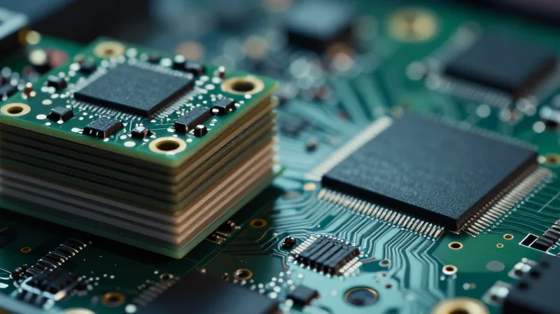
The Limitations of Traditional Multilayer Boards
Traditional multilayer PCBs rely on a foundational stack-up architecture where through-hole vias connect specific layers. For decades, this approach served as the industry standard, providing sufficient interconnect density for desktop computing and industrial applications. However, as wearable technology demands increasingly aggressive miniaturization, the reliance on through-hole and standard blind/buried via configurations has become a bottleneck. These traditional boards suffer from restrictive routing channels and significant wasted space, making them incompatible with the high-density interconnect requirements of modern system-in-package (SiP) designs.
Structural Scaling Constraints
The primary issue with legacy board architecture is the physical footprint required by standard via structures. Traditional through-hole vias pass through every layer, essentially 'stabbing' through the entire board and consuming valuable surface area on every internal plane. This creates a geometric limit on routing density. In contrast, Any-Layer HDI architecture employs microvias that can transition between any two adjacent layers, effectively eliminating the need for through-holes and allowing for a vastly more efficient utilization of the board's Z-axis.
| Feature | Traditional Multilayer | Any-Layer HDI |
|---|---|---|
| Via Structure | Through-hole/Blind/Buried | Every-layer Microvias |
| Routing Density | Low to Moderate | Ultra-High |
| Design Footprint | Large/Extensive | Minimized/Compact |
| Wearable Suitability | Limited | Optimal |
Technical FAQ
- Why can't traditional boards handle modern wearable demands?
Traditional boards require larger spacing for through-hole drilling and lack the vertical interconnect density needed to support the high pin-count ICs found in miniaturized smartwatches and health trackers. - How does Any-Layer HDI change the routing paradigm?
By allowing connections between any two adjacent layers via laser-drilled microvias, Any-Layer HDI enables designers to route signals through the stack-up with near-total freedom, significantly reducing the required board area.
Understanding the Any-Layer HDI Advantage
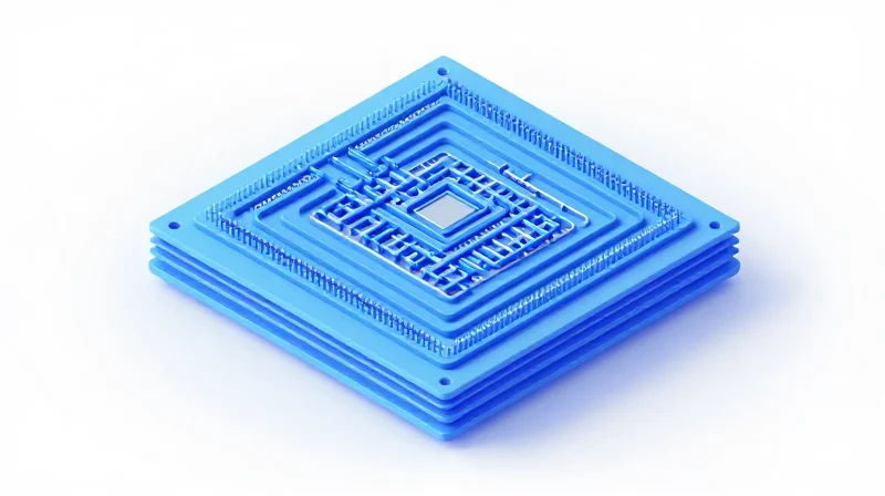
Defining Any-Layer HDI Architecture
Any-Layer High-Density Interconnect (HDI) technology, often referred to as Any-Layer Via (ALV) construction, represents the pinnacle of contemporary PCB design. Unlike traditional multilayer boards that rely on sequential lamination and laser-drilled microvias confined to specific layer pairs, Any-Layer HDI permits the formation of conductive copper vias between any two layers within the stack-up. This capability effectively removes the constraints imposed by buried and blind via structures, allowing for a completely flexible and dense vertical interconnection network.
The Proprietary Process Advantage
The fabrication of Any-Layer HDI relies on advanced additive and semi-additive processing (SAP) techniques. By utilizing conductive paste filling or specialized laser ablation and copper plating, manufacturers can create a seamless vertical structure that connects every single layer to its neighbor. This allows for significantly higher component density and shorter signal paths, which are critical for high-frequency signal integrity in space-constrained wearable devices.
| Feature | Traditional Multilayer | Any-Layer HDI |
|---|---|---|
| Via Placement | Layer-pair specific | Any layer combination |
| Routing Density | Moderate | Ultra-high |
| Board Footprint | Standard | Reduced by 30-50% |
| Signal Integrity | Limited by via stubs | Superior due to shorter paths |
Common Questions Regarding HDI Implementation
- Why does Any-Layer HDI improve wearable performance?
The ability to route signals directly between adjacent layers reduces trace length and parasitic capacitance, which are essential for low-power, high-speed data transmission in miniature devices. - Is Any-Layer HDI cost-effective for mass production?
While the initial unit cost is higher than traditional boards due to complex laser drilling and plating cycles, the reduction in total board layers and PCB area often results in a lower system-level cost. - Does this technology impact signal integrity?
Yes, positively. By minimizing via stub length, Any-Layer HDI significantly reduces signal reflections and electromagnetic interference, making it ideal for the high-frequency requirements of 5G and Bluetooth-enabled wearables.
Space Efficiency and Miniaturization
Architectural Benefits of Any-Layer HDI
Traditional multilayer boards rely on through-hole or buried via technology, which consumes significant internal real estate. In contrast, Any-Layer HDI utilizes laser-drilled microvias that can connect any two conductive layers. This structural flexibility allows designers to transition signals vertically through the board, effectively 'stacking' components on both sides of the PCB without the footprint penalties associated with via-in-pad or massive drill keep-out zones.
Space Optimization Metrics
| Feature | Traditional Multilayer | Any-Layer HDI |
|---|---|---|
| Via Routing | Layer to Layer fixed | Inter-layer flexibility |
| Board Footprint | Larger due to drilling | Up to 40% reduction |
| Component Density | Low to Moderate | Ultra-High |
| Design Complexity | Low | High |
Frequently Asked Questions
- How does Any-Layer HDI specifically benefit small wearables?
By allowing dense routing in all vertical layers, it frees up peripheral board area for larger batteries or specialized sensors that were previously impossible to fit in the same housing. - Does the increased density lead to thermal bottlenecks?
While density is higher, the inclusion of microvias often improves vertical thermal conductivity, provided the stack-up is balanced during the design phase. - Is the transition from multilayer to Any-Layer worth the cost for low-volume devices?
For specialized medical or flagship wearables where size is the primary value proposition, the unit cost premium is usually offset by the reduction in housing material and system miniaturization gains.
Performance and Signal Integrity Benefits

Optimizing Signal Integrity through Interconnect Efficiency
In traditional multilayer PCBs, the reliance on through-hole vias creates long stubs that act as antennas, introducing significant signal reflection and electromagnetic interference (EMI). Any-Layer HDI mitigates these effects by utilizing micro-vias for point-to-point connections, drastically shortening trace lengths and minimizing parasitic inductance and capacitance. This precise routing architecture is essential for wearables that must process high-frequency signals with minimal latency.
Performance Metrics Comparison
| Feature | Traditional Multilayer | Any-Layer HDI |
|---|---|---|
| Via Stub Length | High (significant resonance) | Negligible/Zero |
| Signal Propagation | Delayed/Higher Impedance | Optimized/Stable |
| Thermal Path | Obstructed by through-holes | Direct/Continuous |
| EMI Susceptibility | High | Low |
Advanced Thermal Management
Wearable devices face chronic thermal challenges due to their constrained form factors and proximity to human skin. Any-Layer HDI offers a superior thermal management pathway compared to standard boards. By utilizing stacked micro-vias, heat can be transferred efficiently from internal power components directly to thermal dissipation planes or external copper layers. This architectural flexibility prevents local hot spots and ensures the long-term reliability of sensitive sensors and microcontrollers.
Technical FAQs
- How do micro-vias reduce latency?
Micro-vias provide direct vertical connectivity between adjacent or specific layers, reducing the total electrical path length and ensuring faster signal propagation times. - Does Any-Layer HDI help with high-speed data protocols?
Yes, it enables tighter impedance control and reduced discontinuity, which are critical for maintaining signal integrity in high-speed protocols like MIPI or USB 3.0. - Is the thermal management better than copper coins?
While copper coins are effective, Any-Layer HDI provides superior distributed thermal relief, allowing heat to escape through a complex web of micro-vias rather than relying on a single, heavy, and localized thermal slug.
Addressing Reliability and Thermal Constraints
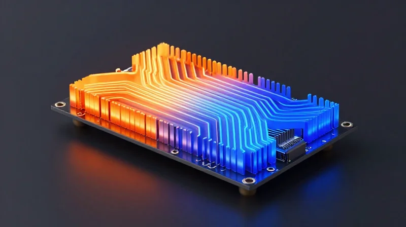
In the confined, high-stress environments of modern wearables, standard multilayer PCBs often fall short due to the structural weaknesses introduced by conventional through-hole drilling. Any-Layer HDI (High-Density Interconnect) technology fundamentally shifts this paradigm by utilizing a via-in-pad structure and stacked microvias, effectively replacing intrusive through-holes with compact, reliable vertical interconnects. This architectural evolution not only prevents common failure points associated with barrel cracking but also creates a more contiguous copper path for heat transfer.
Mechanical Robustness Through Via Optimization
The removal of through-holes eliminates the mechanical stress concentrators that plague traditional boards during thermal cycling. Traditional holes pass through the entire substrate, acting as weak links; in contrast, Any-Layer HDI structures provide superior interlaminar bond strength and improved resistance to mechanical vibration and shock, which are constant factors in wearable ergonomics.
Thermal Management Comparisons
| Feature | Traditional Multilayer | Any-Layer HDI |
|---|---|---|
| Via Structure | Mechanical Through-Hole | Stacked Microvias |
| Thermal Resistance | Higher due to voids | Lower due to solid copper stacks |
| Reliability under Stress | Prone to barrel cracking | High structural integrity |
| Heat Dissipation Path | Indirect and segmented | Direct vertical heat sinking |
Key Considerations for Thermal Stability
- How does stacking microvias assist in cooling?
Stacked microvias create a solid, continuous copper thermal conduit from internal components to external surface layers, significantly shortening the distance heat must travel to reach a heat sink or the device casing. - Can Any-Layer HDI mitigate hotspots?
Yes. By allowing high-density signal routing and component placement flexibility, designers can distribute power consumption more evenly across the board, preventing localized thermal stress. - Why is reliability critical in wearables?
Wearables are subject to frequent thermal expansion and contraction cycles caused by battery heat and skin proximity; the enhanced ductility of HDI structures resists the fatigue that eventually fails traditional via barrels.
Cost-Benefit Analysis for High-Volume Production
The Economics of High-Volume HDI Implementation
Transitioning to Any-Layer HDI technology represents a strategic pivot where upfront capital expenditure is traded for significant gains in assembly yield, space optimization, and product performance. While individual board costs for Any-Layer HDI are higher due to complex laser drilling and sequential lamination processes, the total cost of ownership often decreases at scale through reduced device failure rates and shortened design-to-market cycles.
| Metric | Traditional Multilayer | Any-Layer HDI |
|---|---|---|
| Unit Manufacturing Cost | Low | High |
| Assembly Failure Rates | Moderate/High | Low |
| Design Density | Limited | Ultra-High |
| Overall BOM Optimization | Neutral | High (Reduced layers) |
Key Financial Considerations for Wearables
- Does the higher cost of HDI justify the ROI in wearable consumer devices?
Yes, for high-volume wearables, the cost of HDI is offset by the ability to fit more functionality into a smaller enclosure, which increases market value, alongside a reduction in PCB layer count which simplifies the assembly process. - How does HDI improve manufacturing yield compared to traditional boards?
By eliminating complex through-hole vias that act as thermal and stress weak points, HDI reduces post-assembly rework and field failures, leading to a higher 'first-pass yield' and reduced total warranty costs. - Are there long-term cost benefits to standardizing on HDI?
Standardizing allows for a consistent design library that accelerates future product iterations, effectively lowering the R&D and prototyping costs over a multi-year product roadmap.
Ultimately, the shift to Any-Layer HDI should be viewed not just as a component cost increase, but as an efficiency investment. Manufacturers who prioritize the reduction of physical board footprint and signal latency gain a competitive edge that justifies the initial premium in the highly crowded wearable tech sector.
Design Considerations for Modern Engineers
Strategic Design Transitions for Any-Layer HDI
Transitioning from standard multilayer PCBs to Any-Layer HDI requires moving away from conventional routing mentalities. Designers must prioritize 'interconnect-first' layouts where microvias are treated as primary structural elements rather than afterthoughts. This evolution demands a shift toward laser-drilled blind and buried vias, which provide the flexibility to route high-density components on any layer, effectively eliminating the bottleneck of traditional through-hole vias.
| Design Factor | Traditional Multilayer | Any-Layer HDI |
|---|---|---|
| Via Structure | Through-hole | Stacked/Staggered Microvias |
| Routing Density | Moderate/Limited | Ultra-high (Any-layer access) |
| Signal Path | Long/Indirect | Short/Optimized |
| Stack-up Complexity | Fixed/Static | Dynamic/Sequential |
Material Selection and Thermal Management
In wearable applications, material choice is non-negotiable. Designers must select substrates with high glass transition temperatures (Tg) and low coefficient of thermal expansion (CTE) to withstand the sequential lamination process inherent in Any-Layer HDI. Utilizing laser-direct-structuring (LDS) compatible materials or high-frequency low-loss laminates helps maintain signal integrity while managing the increased heat concentration resulting from smaller form factors.
- How does HDI influence component placement?
Any-Layer HDI allows for 'via-in-pad' technology, enabling components to be placed directly over vias, which significantly shrinks the required board surface area. - What is the primary constraint of microvia stacking?
Over-stacking microvias can lead to thermal stress points; engineers should alternate between stacked and staggered via configurations to improve mechanical reliability. - Is impedance control more difficult in HDI?
Yes, because the narrower trace widths and tighter coupling required in HDI demand precise dielectric thickness control during the lamination process.
Future-Proofing Your Hardware Strategy
The Strategic Shift Toward HDI Dominance
Future-proofing a hardware strategy requires moving beyond the constraints of traditional multilayer PCB architectures. As wearable technology evolves toward smaller form factors with higher sensor density, the reliance on standard through-hole plating becomes a bottleneck to innovation. Transitioning to Any-Layer HDI allows engineers to reclaim significant board real estate, facilitating the integration of advanced battery technologies and sophisticated biometric sensors that are impossible to accommodate on legacy substrates.
Comparative Strategic Outlook
| Strategic Metric | Traditional Multilayer | Any-Layer HDI |
|---|---|---|
| Product Lifecycle | Short-term capacity | Long-term scalability |
| Design Complexity | Restricted routing | Density optimized |
| Market Adaptability | Low agility | High agility |
| Component Density | Legacy standard | Future-proof high |
FAQs on Long-Term Hardware Strategy
- Is the investment in HDI justified for lower-tier wearable products?
While traditional boards are cheaper upfront, the cost of iterative redesigns for HDI-enabled components often outweighs the initial material savings, making Any-Layer HDI a superior long-term investment for brand consistency. - How does HDI support future sensor integration?
By removing through-hole interference, Any-Layer HDI provides clean routing paths that minimize signal noise, which is critical for the high-precision data required by next-generation health monitors. - When is the optimal time to transition from multilayer to HDI?
Transition should occur at the start of a product lifecycle refresh when component density requirements force a trade-off between battery size and PCB area; waiting until a project is mid-cycle risks expensive board re-spins.
Ultimately, the shift to Any-Layer HDI is a commitment to performance density. Companies that prioritize these manufacturing methodologies today will possess the structural flexibility to pivot as wearable technology trends move toward AI-integrated edge computing and ultra-compact medical devices.
The transition to Any-Layer HDI represents more than just a design change; it is a fundamental shift toward the next generation of compact, powerful electronics. By embracing this technology, designers can overcome traditional space constraints and push the boundaries of what wearable devices can achieve. Ready to optimize your next project? Contact our engineering team today to discuss your PCB design requirements and integration strategy.
