As BGA pitches shrink and HDI stackups grow more complex, placing decoupling capacitors has become increasingly difficult.
This article breaks down the root causes and provides systematic solutions.
Decoupling capacitors provide local charge during transient current demands. Closer placement means lower loop inductance and better power integrity (PI).
General guidelines:
Place within 1–2mm of IC power pins
Minimize current loop area
Shorten via and trace lengths
Poor placement leads to:
Increased power noise
Voltage droop
Reduced timing margins
Worse EMI
BGA fanout requires vias, which occupy the space between solder balls — the same area ideal for decoupling capacitors. This creates a structural constraint: designers must trade off between signal fanout and PDN performance.
When the ball pitch shrinks to 0.65mm, dog-bone fanout may still be viable — though tight. Once the pitch drops below 0.5mm, via-in-pad becomes the only practical option.
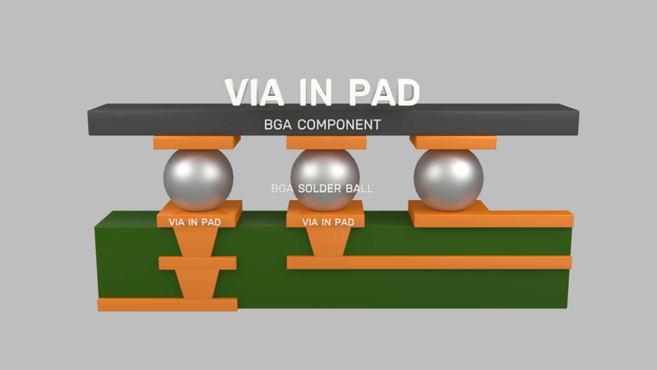
Via-in-pad frees up space between balls by placing vias directly through BGA pads, allowing room for decoupling capacitors. However, this comes at a cost: filled and plated microvias and sequential lamination are required, significantly increasing manufacturing complexity.
It is critical to recognize that via-in-pad does not solve the decoupling problem — it merely relocates it. Freeing up center space removes one constraint, but the remaining surface area may still be insufficient to accommodate the number and value of capacitors required by the PDN.
When this happens, the solution is not simply to add more via-in-pad connections. Designers may need to switch to smaller packages (e.g., 0201 or 01005), redistribute capacitors across different layers, or in extreme cases, evaluate alternative IC packages with different pinouts or ball pitches to better meet PDN requirements.
Decoupling effectiveness at high frequencies is determined by loop inductance — from capacitor, through vias to planes, and back. Loop area depends on via separation and distance to planes.
In HDI stackups, power planes are often split, increasing PDN impedance and exacerbating simultaneous switching noise (SSN) and ground bounce. If power and ground planes are separated by signal layers, decoupling effectiveness drops significantly.
When multiple outputs switch simultaneously, transient currents create voltage fluctuations on power and ground paths. This is worse in HDI because:
Power planes are divided, reducing distributed capacitance
Decoupling capacitors must work harder
Poor placement or high via inductance consumes noise budget quickly
For FPGAs and high-speed processors with hundreds of I/O pins switching at once, proper decoupling around I/O power rails is as important as core power decoupling.
HDI designs are dense by definition. The conflict is between:
PDN-required decoupling capacitor count
Space consumed by signal routing, thermal vias, connectors, and mechanical constraints
Core voltages can be as low as 0.8V with transient currents reaching hundreds of amps. Target impedance must be below 1mΩ to suppress ripple. This requires careful planning of bulk caps, HF decoupling, and interlayer capacitance — all competing for limited space.
A "Correct-by-Design" approach is required: pre-layout PDN simulation to establish target impedance and capacitor count, followed by post-layout verification.
| Type | Typical Values | Placement Priority |
|---|---|---|
| High-Frequency | 0.01μF / 0.047μF / 0.1μF | Closest to IC — distance and via inductance have greatest impact |
| Mid-Frequency | 1μF / 2.2μF / 4.7μF | Near IC, but lower priority than HF caps |
| Bulk Capacitors | 10μF / 22μF / 100μF | Can be farther away — provide low-frequency energy |
In HDI layouts, premium space near the IC is extremely limited. Small-value HF capacitors must be prioritized — their effectiveness degrades rapidly with distance and via inductance.
For circuits above 1GHz, via inductance is as important as capacitor parasitic parameters. Ideally, the two vias should be placed close together, oriented oppositely to minimize loop area, and connected directly to the nearest plane.
Couple power and ground planes tightly with spacing of ≤4 mils (0.1mm). This reduces dependence on precise capacitor placement, as planes provide distributed capacitance.
Place capacitors symmetrically around ICs with multiple power pins to balance current distribution and reduce EMI.
If top-side space is limited, place caps on the bottom side directly under the IC with vias connecting them. This minimizes loop length.
When surface space is exhausted, embedded capacitance integrates decoupling into PCB layers, saving space while improving electrical performance. Loop inductance approaches zero.
Low-frequency: discrete bulk capacitors
Mid/high-frequency: embedded capacitance in PCB or package
Ultra-high-frequency: on-die capacitance
Each tier covers frequencies others cannot. Offloading mid-frequency decoupling to embedded layers frees valuable surface space.
HDI technologies like via-in-pad don't eliminate constraints — they change where they manifest. When decoupling has no viable space, reassess package, strategy, or embedded options.
PDN simulation is not optional. Run it before placement is locked, treating plane positioning and capacitor count as a unified system.
Tiered placement is key. Place HF, small-value caps closest to the IC; bulk caps can be farther away.
When decoupling issues surface late in HDI designs, available solutions are severely limited. Manage PDN as a core design object from the start.
Need HDI PCB design or manufacturing support?
AnyPCBA has extensive HDI experience, supporting blind/buried vias, via-in-pad, and sequential lamination.
Contact our engineering team →




