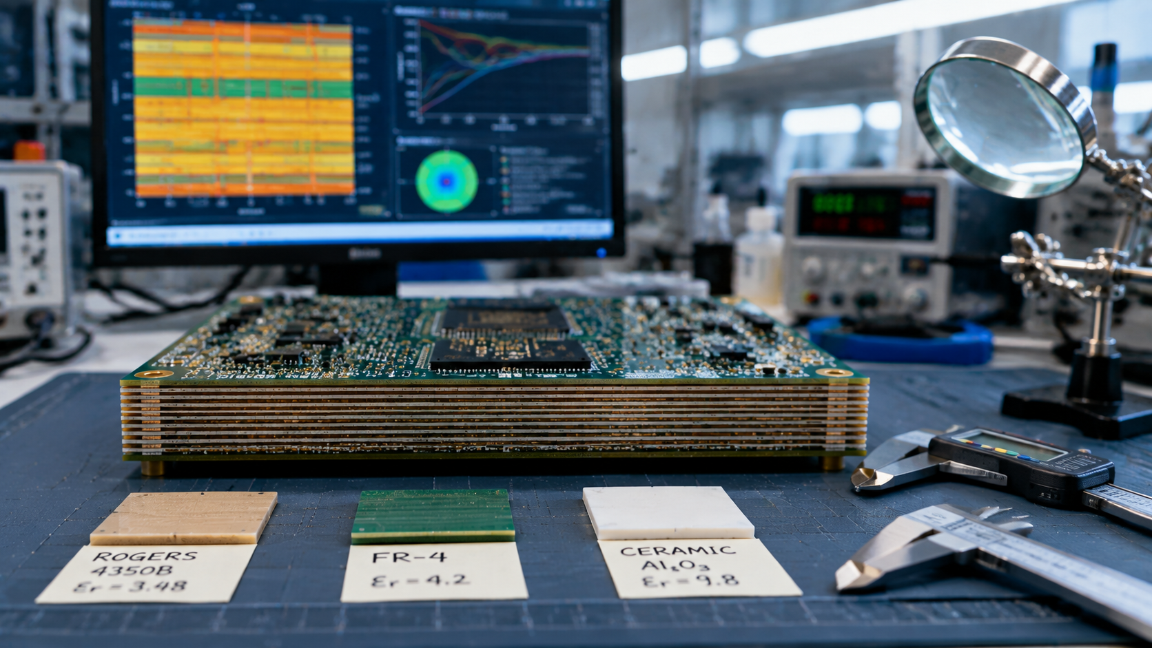
Multilayer printed circuit boards (PCBs) have become the backbone of modern electronic devices. By stacking multiple conductive and insulating layers, they enable complex signal routing, efficient power distribution, and significant space savings — making them essential for applications ranging from smartphones to 5G base stations and electric vehicles.
This guide provides a technical overview of multilayer PCB technology, covering material selection, manufacturing processes, application-specific design considerations, and industry trends.
Smartphones, wearables, and other portable devices demand PCBs that are both ultra-thin and highly integrated. A typical 6-layer board for a flagship phone must fit RF signal layers, application processor power distribution, and sensor control circuits within a 0.8mm thickness — using blind and buried vias to achieve pad pitches below 0.4mm.
Design challenge: Maintaining signal integrity at 5G mmWave frequencies (28GHz) while minimizing board thickness.
Solution approach: HDI (High-Density Interconnect) technology with sequential lamination, enabling 10-layer boards with < 1dB insertion loss at 28GHz and up to 25% board area reduction.
Automotive applications — particularly battery management systems (BMS), domain controllers, and ADAS sensors — require PCBs that operate reliably across extreme temperatures (-40°C to 125°C) while resisting vibration and humidity for 10+ years.
Design challenge: Ensuring stable performance under continuous thermal cycling and high-voltage conditions.
Solution approach: High-Tg FR-4 materials (TG ≥ 170°C), hybrid lamination with Rogers substrates for 77GHz radar, and ENIG surface finish. Key reliability metrics include < 5% insulation resistance drop after 85°C/85% RH testing and ±0.1° radar detection accuracy through controlled impedance layers.
5G base stations and data center switches push PCB technology to its limits. Massive MIMO antenna arrays use 16-layer hybrid boards, with up to 4 layers of high-frequency material (e.g., Rogers 4350B) dedicated to 28GHz signal transmission.
Design challenge: Maintaining phase consistency across 128+ channels with minimal insertion loss and VSWR.
Solution approach: Tight impedance control (≤ ±5% for 100Ω differential pairs), low-roughness copper foil (Rz ≤ 3μm), and full-wave simulation (HFSS) for critical RF paths. Achievable performance: insertion loss ≤ 0.65dB/inch, VSWR < 1.15, channel-to-channel phase error < ±1.5°.
Satellite payloads and missile guidance systems demand PCBs that survive space radiation, extreme temperatures (-196°C to 125°C), and high vibration. Ceramic substrates (Al₂O₃, AlN) combined with metal heat-spreading layers provide the necessary thermal conductivity (> 200W/(m·K)) and mechanical stability.
Design challenge: Managing heat dissipation in high-power computing modules while maintaining signal integrity under EMP exposure.
Solution approach: Vacuum brazing for layer interconnection, embedded passive components (buried resistors), and rigid-flex constructions for 3D packaging. These techniques enable up to 30% board area reduction and enhanced EMP immunity.
Choosing the right base material is the first critical decision in multilayer PCB design. The table below summarizes common material types and their applications:
| Material Type | Typical Grades | Key Parameters | Primary Applications |
|---|---|---|---|
| Standard FR-4 | FR-4 (TG 135-170°C) | Dk 4.2-4.7, low cost | Consumer electronics, industrial controls (< 1GHz) |
| High-Tg FR-4 | High-Tg (TG ≥ 170°C) | Higher thermal stability | Automotive, industrial, high-reliability |
| High-Frequency | Rogers RT/duroid 5880, Taconic TLY-5 | Dk ~2.2, tanδ < 0.0012, low loss | 5G, radar, microwave, high-speed digital |
| Ceramic Substrates | Al₂O₃, AlN | Thermal conductivity 170-240 W/(m·K) | Power modules, aerospace, high-thermal applications |
Precision manufacturing is what makes complex multilayer designs viable. Key processes and their typical specifications include:
| Process | Technology & Specification | Achievable Precision |
|---|---|---|
| Circuit Patterning | LDI (Laser Direct Imaging) | 3/3 mil (0.076mm) line/space, defect rate < 0.05% |
| Lamination | Vacuum press with stepped temperature/pressure profile | Layer bond strength ≥ 1.5N/mm, dielectric uniformity error < 2% |
| Drilling | Laser drilling for microvias | 0.05mm microvias, wall roughness Ra ≤ 2.5μm |
| Impedance Control | HFSS simulation + dynamic compensation, pulse plating | 100Ω differential impedance tolerance ≤ ±5% |
| Layer Alignment | X-Ray inspection, automated optical registration | ±5μm alignment precision for 12+ layer boards |
A well-designed multilayer PCB must balance electrical performance with manufacturability and testability. Key DFM considerations include:
Symmetry: Keep the stackup symmetrical around the center to prevent board warping during lamination.
Reference planes: Ensure high-speed signal layers have adjacent solid ground or power planes for controlled impedance and return current paths.
Material compatibility: When mixing materials (e.g., Rogers + FR-4), account for different coefficients of thermal expansion (CTE).
Thermal vias: Use arrays of plated vias under power components to conduct heat to internal or bottom-side copper planes.
Copper balance: Distribute copper evenly across each layer to avoid hot spots and uneven heating during reflow soldering.
Test point placement: Add dedicated test points on a 100-mil grid for ICT (In-Circuit Testing) to achieve ≥ 95% net coverage.
Accessibility: Ensure test points are accessible from the same side of the board where possible.
The evolution of 6G (target frequencies > 100GHz), AI chips with 3D packaging, and autonomous vehicles is driving several key trends in multilayer PCB technology:
| Trend | Technology Direction | Expected Impact |
|---|---|---|
| Higher Density Integration | SLP (Substrate-Like PCB), embedded passives (buried resistors/capacitors) | Line/space down to 2-3 mil, passive components integrated into board layers |
| Ultra-Low Loss Materials | Hydrocarbon-based laminates, PTFE blends | Dk ≤ 2.0, tanδ < 0.001 for 0.1-1THz applications |
| Smart Manufacturing | Digital twins, AI-driven process control, blockchain traceability | Real-time process optimization, full material and production traceability |
Multilayer PCB technology continues to evolve at a rapid pace, driven by the insatiable demand for smaller, faster, and more reliable electronic systems. Understanding the fundamentals of material selection, manufacturing processes, and application-specific requirements is essential for engineers looking to push the boundaries of their designs.
At AnyPCBA, we combine ISO 13485 and IATF 16949 certified manufacturing with deep technical expertise to support projects from prototype to production. Whether you're designing for automotive, 5G, or high-performance computing, our engineering team can help optimize your multilayer PCB for manufacturability, reliability, and cost.
Need support for your multilayer PCB project?
Contact our technical team →




