9 PCB Layout Tips Every Advanced Engineer Knows (But Beginners Might Not)
Today, I'm excited to share PCB design tips that can significantly improve your designs.
1. Regulator Layout
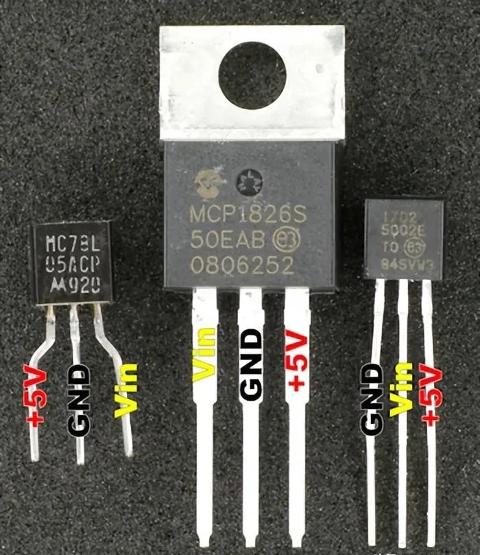
Linear regulators are common components consisting of three pins:
- Output voltage (e.g., 5V, 3.3V)
- Ground (GND)
- Unregulated input voltage
Pin order and packaging can vary across different models, so pay close attention during design.

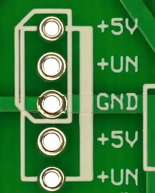
If you layout your PCB thoughtfully, swapping out regulators later for higher input voltages or lower dropout voltages becomes much easier.

Add a 4th and 5th hole with the following pin arrangements:
- +5, +UN, GND (top three holes)
- GND, +UN, +5 (top three holes reversed)
- +UN, GND, +5 (middle three holes)
- +5, GND, +UN (middle three holes reversed)
- GND, +5, +UN (bottom three holes)
- +UN, +5, GND (bottom three holes reversed)
With a diameter of 0.040 inches for all holes, this will accommodate TO-220 and TO-92 packages.
2. Compatibility of Different Trimmer Potentiometer Pins
Trimmer potentiometers come in various package styles, with the most common having a 0.1-inch lead spacing. However, the lead connections may not align neatly with the body.
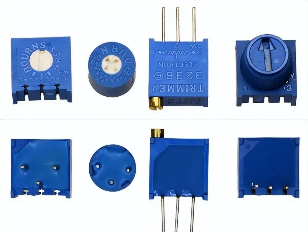
To ensure compatibility, design a 3x3 grid pattern that can accommodate multiple types of potentiometers in the same PCB location.
3. Capacitor Layout - Add Extra Holes
Utilizing three capacitor holes allows you to choose between 0.1-inch and 0.2-inch spacing during assembly.
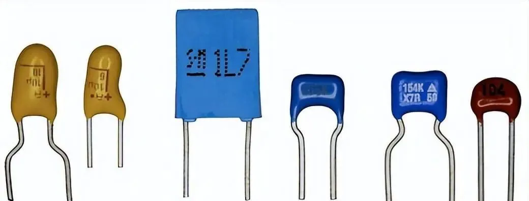
Make the first pad square and positive, while grounding the other two pads. This way, even if you use different capacitor sizes, the smallest component will align with the first pad.
Extra holes also provide a backup grounding connection in case of errors on the PCB.
4. Button Layout - Add Extra Holes
Tactile buttons are common in electronics, typically with four pins arranged in a square.

To ensure proper installation, consider adding three extra holes in the center to allow for various button types.

5. Wider Round Pads Around Holes
Most PCB layouts use a 0.056-inch pad around a common 0.029-inch hole. This works well for DIP chips but may not be suitable for wider hole spacing.
Adding larger round pads around wider holes maximizes contact area during soldering.
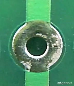
6. Solder Mask Layer
The solder mask layer provides electrical and chemical insulation, protecting metal traces from environmental damage and accidental shorts.
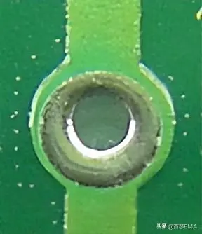
Be cautious that extended pad areas may get covered by the solder mask during PCB production.
7. Copper Fill to Reduce Heat and Improve Efficiency
Some components, like voltage regulators and motor drivers, generate heat. A simple method to dissipate heat is to place copper fills beneath these chips, which can enhance performance.
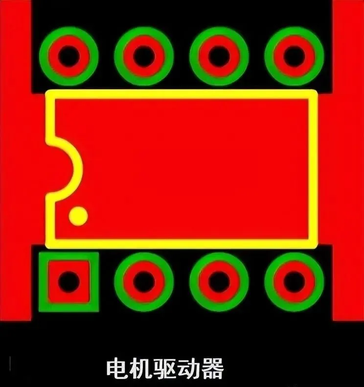
However, ensure there’s enough routing space, as sometimes you can't add a copper plane beneath the chip.
8. Test Point Design
When measuring DC voltages, ensure that your ground probe connects to the same ground as your circuit. Place test points on the PCB edge to avoid dangling wires.
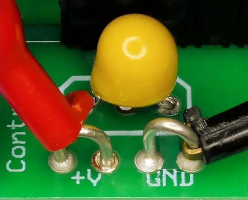
Using slightly larger holes (0.035 inches) for test point connections will facilitate easier access for probes.
9. Ground and Power Line Design
Ground and power lines should be thicker than signal lines. Thicker traces not only carry more current but also visually distinguish power lines from signal lines, reducing the risk of connecting power incorrectly to signal pins.
 AnyPCBA