The Art and Science of NAND Gate Layout: A Practical Guide
NAND gates are a fundamental element in digital circuit design. The efficiency and performance of complex VLSI circuits are directly impacted by the physical layout of these basic gates. This article provides a comprehensive overview of NAND gate layout, from basic principles to advanced techniques, and highlights best practices for successful layout design for both manual and CAD methodologies. The proper use of this building block is at the center of the digital age that we currently live in.
Basics of NAND Gate Function and Logic
The NAND gate, a cornerstone of digital logic, performs the inverse of an AND operation. Its output is logic HIGH (1) if any of its inputs are LOW (0), and logic LOW (0) only when all inputs are HIGH (1). This fundamental behavior makes NAND gates universal; they can be configured to implement any other logic gate including AND, OR, and NOT. This universality, alongside the relative simplicity of its CMOS implementation, solidifies its prevalence in digital circuit design.
| Input A | Input B | NAND Output |
|---|---|---|
| 0 | 0 | 1 |
| 0 | 1 | 1 |
| 1 | 0 | 1 |
| 1 | 1 | 0 |
CMOS Implementation of the NAND Gate
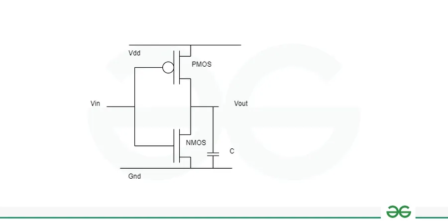
The CMOS (Complementary Metal-Oxide-Semiconductor) implementation of a NAND gate leverages the properties of both PMOS (P-channel MOSFET) and NMOS (N-channel MOSFET) transistors to achieve the desired logic function. This configuration provides a robust and low-power solution for digital circuit design, using a pull-up network with PMOS transistors and a pull-down network with NMOS transistors, working together to perform the NAND logic operation.
| Component | Function | Description |
|---|---|---|
| PMOS Transistors | Pull-Up Network | Connected in parallel, these transistors pull the output high when both inputs are low. |
| NMOS Transistors | Pull-Down Network | Connected in series, these transistors pull the output low when both inputs are high. |
| Input A | Gate Input | Control gate voltage applied to one set of PMOS and NMOS devices |
| Input B | Gate Input | Control gate voltage applied to the other set of PMOS and NMOS devices |
| Output | Gate Output | The output of the circuit; it reflects the NAND operation of A and B. |
In a CMOS NAND gate, the PMOS transistors are connected in parallel between the power supply (Vdd) and the output, forming the pull-up network. Conversely, the NMOS transistors are connected in series between the output and ground (GND), forming the pull-down network. When both inputs (A and B) are high (logic 1), both NMOS transistors turn ON, creating a path to ground and pulling the output LOW (logic 0). Conversely, if either or both inputs are low (logic 0), at least one PMOS transistor will turn ON, thus pulling the output HIGH (logic 1).
Step-by-Step Guide for Manual NAND Gate Layout
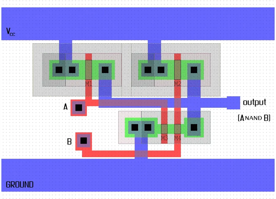
Creating a manual layout for a NAND gate involves a methodical process of placing transistors and interconnecting them via metal layers. This section provides a step-by-step guide to achieve this, emphasizing precision and adherence to design rules.
- Transistor Placement
Begin by placing the two NMOS transistors in series and the two PMOS transistors in parallel. Align transistors to minimize routing distance. Ensure adequate spacing between devices as dictated by the Design Rule Check (DRC). - Well and Substrate Contacts
Add well contacts for PMOS transistors and substrate contacts for NMOS transistors to ensure proper biasing. These contacts are crucial for preventing latch-up and ensuring reliable device operation. - Gate Connections
Connect the gates of the corresponding NMOS and PMOS transistors. Both inputs of the NAND gate should be tied to the gates of the series NMOS transistors and the gates of the parallel PMOS transistors respectively. - Metal Routing for Power
Use metal layers to route VDD to the PMOS transistors and GND to the NMOS transistors. Employ sufficient metal width to minimize resistance and electromigration issues. - Metal Routing for Output
Route the output by connecting the drains of the parallel PMOS transistors and the drains of the series NMOS transistors at the output node of the NAND gate. - Input Routing
Route the inputs to the corresponding gates using metal layers. Connect the inputs to the gate terminals of both PMOS and NMOS transistor pairs. - Contact and Via Placement
Implement contacts between transistor terminals and metal layers, as well as vias between different metal layers. This ensures that signal integrity and proper functionality.
Optimizing Transistor Sizing and Geometry for Performance
Optimizing transistor sizing and geometry in a NAND gate layout is crucial for achieving desired performance metrics such as switching speed, driving strength, and power consumption. The core challenge involves balancing these often competing factors to create a robust and efficient design. This section will delve into techniques for determining optimal transistor dimensions.
| Parameter | Description | Impact on Performance |
|---|---|---|
| Channel Width (W) | The lateral dimension of the transistor's channel. | Directly affects the drive current. Wider channels provide higher current but increase capacitance. |
| Channel Length (L) | The length of the transistor's channel, between source and drain. | Impacts the speed and current. Shorter channels increase current, however, it can also lead to increased leakage and short-channel effects. |
| Oxide Thickness (Tox) | The thickness of the gate dielectric layer. | Thinner oxides increase the gate capacitance, potentially increasing speed but also increasing gate leakage. |
| Number of fingers (NF) | A layout technique that divides the transistor into multiple parallel devices. | Used to manage layout area and reduce resistance per unit width. This enables finer control over transistor geometry. |
The sizing of PMOS and NMOS transistors in a CMOS NAND gate is critical because they have different mobility characteristics. NMOS transistors, which are responsible for pulling the output to ground, have higher mobility than PMOS transistors, which pull the output to VDD. Therefore, PMOS transistors typically require wider channels than their NMOS counterparts to achieve balanced rise and fall times.
To optimize for driving strength, one needs to carefully adjust the W/L ratio. A higher W/L ratio will result in higher drive current, enabling the gate to switch more quickly. This approach, however, increases the gate capacitance and, consequently, power consumption. For power optimization, reducing the transistor size, especially channel width, can limit dynamic power consumption, at the expense of reducing the drive strength. Therefore, one must strategically size transistors based on their function and performance requirements.
CAD Tool Workflow for NAND Gate Layout (Cadence Example)
The shift from manual layout to Computer-Aided Design (CAD) tools is essential for managing the complexity of modern integrated circuits. This section focuses on using Cadence Virtuoso, a leading industry tool, to automate the NAND gate layout process, which increases efficiency and reduces errors compared to manual methods.
- Schematic Capture
Begin by creating the NAND gate schematic in Virtuoso. This involves selecting the appropriate PMOS and NMOS transistors from the library and connecting them according to the NAND gate logic. - Technology File Setup
Ensure the correct technology file for your chosen fabrication process is loaded into Virtuoso. This file contains the design rules necessary for layout. - Automatic Layout Generation
Virtuoso can automatically generate an initial layout based on the schematic. This initial layout can serve as a starting point, with Virtuoso respecting the rules defined in the technology file and placing transistors and contacts based on best practice. - Manual Placement and Routing Adjustments
Refine the automatically generated layout manually by adjusting transistor placement and optimizing routing for area, performance, and manufacturability. This step involves moving or resizing elements, and also adjusting routing to minimize impedance or meet timing requirements. - Design Rule Check (DRC)
Run a DRC check to verify that the layout conforms to the design rules of the selected technology. Correct any violations identified before proceeding, to ensure that the layout is manufacturable. - Layout Versus Schematic (LVS) Verification
Perform an LVS verification to confirm that the layout matches the original schematic. Any discrepancies must be resolved before tape-out. This step is critical to avoid functionality errors. - Extraction and Parasitic Analysis
Use extraction tools to obtain the parasitic capacitances and resistances of the layout. Incorporate these parasitics into simulation to evaluate circuit performance.
Essential Verifications: DRC and LVS Checks
Design Rule Checking (DRC) and Layout Versus Schematic (LVS) are crucial verification steps in the integrated circuit (IC) design process, particularly after the layout of a NAND gate is completed. These checks ensure the physical layout adheres to manufacturing rules and accurately represents the intended circuit, respectively. Failing to perform these checks can result in non-functional or unreliable chips.
Both DRC and LVS are typically performed using specialized Electronic Design Automation (EDA) tools.
| Verification Type | Purpose | Tool Usage | Key Checks |
|---|---|---|---|
| DRC (Design Rule Check) | Ensures layout complies with manufacturing process rules. | Dedicated DRC tool within EDA suite (e.g., Cadence) | Minimum spacing between features, width of metal lines, via size |
| LVS (Layout Versus Schematic) | Verifies layout matches the original circuit schematic. | LVS tool within EDA suite (e.g., Cadence) | Connectivity between transistors, matching component sizes |
DRC is typically run first, as it addresses the geometric constraints imposed by the fabrication process. Common DRC violations include insufficient spacing between features, incorrect metal line widths, and improperly sized contacts. An LVS check, on the other hand, validates that the netlist extracted from the layout exactly matches the original design's netlist. This is critical for functional correctness. Mismatches can arise from misplacement of components or incorrect wiring in layout.
Best Practices for NAND Gate Layout
Achieving an optimal NAND gate layout requires adherence to established best practices that consider routing efficiency, layer selection, and overall design principles. These practices minimize parasitic effects, maximize performance, and ensure design robustness, and they are critical in transforming a functional design into a manufacturable, high-yield integrated circuit.
- Transistor Placement
Place transistors symmetrically to minimize routing lengths and ensure balanced parasitic capacitances. Keep the PMOS and NMOS transistors in close proximity for efficient current flow and reduced area. - Power and Ground Routing
Use wide metal layers for power and ground rails to minimize IR drop and ensure adequate current delivery. Implement a robust power grid to minimize noise and maintain a stable voltage supply. - Interconnect Routing
Minimize routing lengths between transistors, using the shortest path possible. Use vias sparingly to reduce resistance and capacitance. Utilize lower metal layers for local connections and higher layers for longer interconnects. - Layer Selection
Use lower metal layers for local interconnects and higher metal layers for longer interconnects, especially for power and ground rails to decrease resistance and optimize signal integrity. Choosing the correct metal layer will minimize signal delay and ensure reliable operation. - Via Optimization
Minimize the use of vias due to their parasitic resistance and capacitance. However, always add enough vias to maintain connectivity and avoid electromigration issues and improve the reliability of interconnects. Place vias carefully to ensure they are not adding unnecessary resistance. - Guard Rings
Implement guard rings to isolate the NAND gate from adjacent circuits, preventing noise coupling. Ensure the guard rings are properly connected to the appropriate power or ground rails. - Design Rule Checking (DRC)
Always run DRC checks to ensure the layout adheres to the semiconductor manufacturing guidelines, which avoids manufacturing defects. This step is crucial before tapeout. - Layout Versus Schematic (LVS)
Always perform LVS verification to confirm that the layout accurately represents the design schematic, ensuring the layout performs as intended. Use LVS tools to confirm the correctness of layout connections.
Frequently Asked Questions about NAND Gate Layout
This section addresses common questions and concerns related to NAND gate layout, focusing on practical challenges, performance implications, and best practices. These FAQs aim to provide clear answers to assist both novice and experienced designers.
- What are common mistakes to avoid in NAND gate layout?
Common pitfalls include mismatched transistor sizes, insufficient spacing between devices, and improper metal routing. These issues can lead to performance degradation and fabrication failures. Ensuring adequate spacing, adhering to design rules, and matching device parameters are crucial for a robust layout. - How does layout affect the performance of a NAND gate?
Layout significantly impacts performance through parasitic capacitances and resistances. Poorly routed metal can add unwanted resistance, while close proximity of components can increase capacitance, thereby slowing down the circuit. Careful consideration of routing and transistor placement can optimize switching speed and reduce signal delay. - What is the impact of transistor sizing on NAND gate performance?
Transistor sizing affects both driving strength and power consumption. Larger transistors provide more current and faster switching but also increase capacitance and area. Optimizing transistor sizes involves balancing the need for performance against available area and power consumption limits. Appropriate sizing ensures that the NAND gate can drive subsequent loads effectively. - What is the best method for routing metal layers in a NAND gate layout?
Strategic use of metal layers is essential for minimizing resistance and signal delays. Thicker, top-level metals generally have lower resistance and should be used for critical paths. Shorter, direct routing paths, along with minimizing the use of vias, reduces resistance and parasitic capacitance. Avoidance of sharp bends also helps minimize signal reflections. - How do you ensure that the NAND gate layout is DRC and LVS clean?
Design Rule Checking (DRC) verifies the physical layout against technology-specific design rules, while Layout vs. Schematic (LVS) confirms that the layout matches the intended circuit schematic. Running these verifications iteratively throughout the layout process, and fixing identified errors is critical to ensuring the functionality and manufacturability of the design. - Are there specific considerations for NAND gate layout in different technology nodes?
As technology nodes shrink, parasitic effects become more pronounced. In smaller technology nodes, considerations like well proximity effect and metal density become critical. It is important to adhere to specific design rules that are often stricter in advanced process technologies, as well as using more sophisticated modeling and verification tools. - What are some advanced techniques for improving NAND gate layout density?
Techniques like shared contacts, transistor folding, and transistor stacking can be employed to improve layout density. Shared contacts reduce area and capacitance by merging adjacent devices. Transistor folding and stacking allow for the layout of larger transistors with smaller footprints. These techniques, while increasing complexity, improve overall design efficiency and packing density.
Advanced Techniques in NAND Gate Layout
While basic NAND gate layouts serve as a foundation, advanced techniques are essential for achieving higher density, improved performance, and reduced power consumption in complex integrated circuits. These techniques often involve more intricate design considerations and a deeper understanding of semiconductor physics and fabrication processes.
- Shared Contacts
Sharing contacts between adjacent transistors, particularly source/drain contacts, minimizes the area occupied by the gate, leading to a more compact layout. This technique reduces the total number of contacts needed and helps reduce parasitic capacitance. The implementation needs careful consideration of manufacturing variations and related design rules. - Transistor Stacking
Stacking transistors is a technique to reduce the footprint of a circuit by arranging them in a series configuration, and can be used to implement complex logic functions with fewer transistors than traditional approaches. Stacking PMOS and NMOS transistors creates more compact layouts by sharing common terminals, resulting in reduced overall gate area and increased density. This technique, while advantageous in density, requires careful consideration of effects on signal integrity. - Gate Interdigitation
Interdigitation involves arranging transistors with alternating fingers to achieve a balanced transistor layout. Interdigitating PMOS and NMOS transistors, particularly in high performance circuits, helps reduce parasitic resistance and capacitance, resulting in faster switching speeds and improved signal integrity. Proper interdigitation needs to ensure matched performance between transistors and consistent channel width and length. - Multi-Gate Transistors
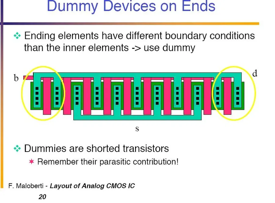
Using multi-gate transistors (e.g., FinFETs) instead of traditional planar transistors improves gate control over the channel, reducing leakage and enabling higher drive currents in a compact footprint. These transistors are more complex to layout and require new design rules and procedures. The adoption of multi-gate technology allows further density improvement with performance increase. - Dummy Fill and Planarization
Adding dummy structures, such as dummy polysilicon or metal, helps maintain the uniformity of the layout across a chip. Dummy fill is added to ensure consistent density across layers, improving manufacturability and reducing issues related to lithography and Chemical-Mechanical Planarization (CMP). This results in fewer defects and enhanced device reliability.
In summary, mastering the intricacies of NAND gate layout is fundamental to achieving efficient and effective VLSI circuit design. Through this guide, we have covered the foundational aspects, manual and CAD approaches, and advanced techniques. Continuous practical application of these skills will ensure that designers can continue to improve their skills, and have a greater appreciation for these basic building blocks of digital logic, and their impact on society.