Choosing the Right PCB Layout Company: A Comprehensive Guide
In today’s tech-driven world, printed circuit boards (PCBs) are the backbone of almost every electronic device. From your smartphone to complex industrial machinery, these intricate boards form the crucial link between components. Selecting the right PCB layout company is a decision that can significantly impact product quality, time-to-market, and cost. Let's delve into what to consider when choosing the ideal partner for your next electronics project.
Understanding Your PCB Layout Needs
Before engaging a PCB layout company, a thorough assessment of your project's specific needs is crucial; this detailed evaluation forms the cornerstone for effective partner selection and successful project execution. This initial step ensures that the chosen company possesses the necessary expertise, resources, and tools to meet your project's requirements accurately, thereby minimizing delays and ensuring a seamless process from design to manufacturing.
- Complexity
Assess the intricacies of your design, considering the number of components, the signal routing challenges, and any special requirements such as impedance control. - Size and Dimensions
Determine the required board dimensions and the physical constraints of the enclosure or final product, which directly impacts layout feasibility. - Component Density
Analyze how densely the components are packed on the board, which will impact thermal management, trace routing, and manufacturing processes. - Layer Count
Specify the number of layers required for signal, power, and ground planes, which significantly impacts cost and design complexity. - Required Certifications
Identify specific industry standards and certifications, such as UL and RoHS, that your design must comply with to ensure market access and product safety.
Key Services Offered by PCB Layout Companies
PCB layout companies provide a suite of essential services that span the entire design and manufacturing process. These services are crucial for translating electronic circuit schematics into physical printed circuit boards ready for fabrication and assembly. Selecting a company offering the right combination of services directly impacts project success, timeline, and cost-effectiveness.
- Schematic Capture
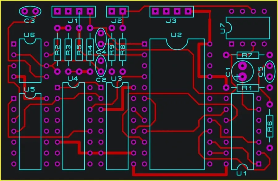
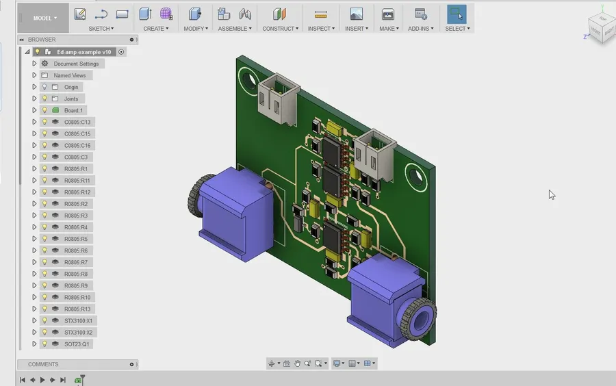
This initial stage involves converting a conceptual circuit diagram into a digital schematic using specialized software. It's the blueprint for the physical board layout, defining electrical connections and component placements. - PCB Layout Design
The core service. Here, the schematic is translated into a physical layout, determining component positioning, trace routing, and layer assignment. It's crucial for ensuring signal integrity, thermal management, and manufacturability. - Design for Manufacturing (DFM) Analysis
DFM checks assess the manufacturability of the PCB design, identifying potential problems that could arise during production. This step helps prevent delays and reduces manufacturing costs by ensuring the design aligns with production processes. - Component Selection and Management
Assisting in the selection of appropriate components based on project requirements and availability. This includes considering cost, lead time, and performance characteristics and managing component libraries. - Signal Integrity Analysis
Analyzing how signals propagate through the PCB to ensure proper performance, preventing reflections, signal degradation, and crosstalk. This is especially important for high-speed and sensitive circuits. - Gerber File Generation
Creating the standardized files (Gerber files) required by PCB manufacturers to fabricate the physical boards. These files contain the layer data necessary for PCB production. - Prototype Assembly Support
Some PCB layout companies provide support for prototype assembly, including component procurement, placement, and testing. This allows designers to test and iterate their designs more rapidly.
Essential PCB Design Tools and Software
The selection of appropriate software is crucial for efficient and accurate PCB layout design. Top-tier PCB layout companies leverage industry-standard software to ensure high-quality results, compatibility, and seamless integration with manufacturing processes. Proficiency in these tools is a key indicator of a company's capability.
| Software | Description | Strengths | Common File Formats |
|---|---|---|---|
| Altium Designer | A comprehensive PCB design suite with schematic capture, layout, and simulation capabilities. | User-friendly interface, powerful routing tools, extensive component library, strong industry adoption. | .PcbDoc, .SchDoc, .Gerber |
| Cadence Allegro | High-performance PCB design software used for complex and high-density designs. | Advanced constraint management, robust signal integrity analysis, suitable for high-speed designs. | .brd, .dra, .art |
| KiCad | Open-source EDA software with a complete suite of tools for PCB design. | Free and open-source, versatile, active community, suitable for a wide range of projects. | .kicad_pcb, .sch, .gerber |
| Eagle | Popular PCB design software known for its ease of use and affordability. | Intuitive interface, extensive community support, suitable for hobbyists and smaller projects. | .brd, .sch |
- Software Compatibility
Confirm that the PCB layout company uses software compatible with your project's requirements and your in-house tools. Standard file format support such as Gerber, ODB++, and IPC-2581 is essential for smooth data exchange and manufacturing processes. - Version Control
Ensure the company maintains good version control practices for their design files, enabling you to track changes and revert to previous design iterations if needed. - Data Migration
If your design needs to be migrated from one software to another, check if the company offers migration support to avoid compatibility issues.
Experience and Expertise in Various Industries
The nuances of PCB design vary considerably across industries, demanding specialized expertise from a PCB layout company. A firm's proven experience within a specific sector directly correlates to its ability to meet the unique challenges and stringent requirements that may be imposed by that sector. Selecting a company with demonstrated experience ensures a smoother design process that complies with relevant standards and specifications.
| Industry | Specific Requirements | Relevant Expertise |
|---|---|---|
| Medical Devices | High reliability, biocompatibility, stringent regulations (e.g., FDA compliance) | Experience with ISO 13485, knowledge of biocompatible materials, robust signal integrity analysis, and adherence to rigorous quality control procedures. |
| Aerospace | Extreme environmental conditions (temperature, vibration), high reliability, low signal noise, strict certification processes (e.g., DO-254) | Expertise in high-speed design, robust grounding techniques, knowledge of materials suitable for harsh environments, and compliance with aerospace industry standards. |
| Consumer Electronics | Cost-effectiveness, high-volume production, compact design, aesthetics, rapid development cycles | Experience in optimizing layouts for cost and manufacturability, expertise in high-density layouts, and capability of handling fast-paced projects. |
| Automotive | High reliability, wide temperature ranges, vibration resistance, compliance with automotive standards (e.g., AEC-Q100) | Expertise in designing for harsh environments, knowledge of automotive-grade components, and understanding of EMI/EMC considerations in automotive applications. |
| Industrial Automation | Robustness, reliability, long operating life, resistance to electrical noise and interference | Experience with designs for harsh industrial conditions, focus on signal integrity and noise reduction, and expertise in long-life cycle product design. |
| Telecommunications | High-speed data transmission, signal integrity, impedance control, low power consumption | Expertise in high-speed digital and RF design, deep understanding of signal integrity and impedance matching, and optimization for low power applications. |
The Importance of Design for Manufacturing (DFM)
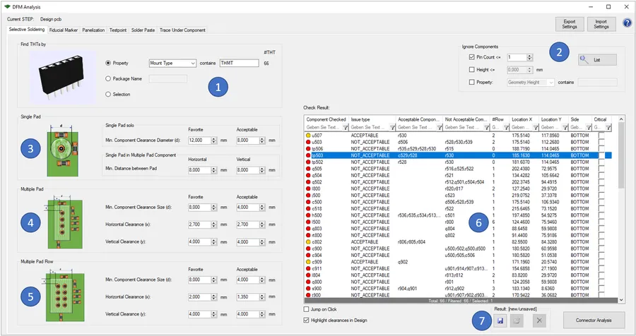
Design for Manufacturing (DFM) is a critical aspect of PCB layout, focusing on ensuring that the design can be efficiently and reliably manufactured. A competent PCB layout company should prioritize DFM analysis, not only to prevent production delays and reduce costs but also to guarantee the final product meets the required performance and reliability standards.
DFM analysis involves assessing the PCB design for potential manufacturing issues. This process takes into account various manufacturing limitations and capabilities, such as minimum trace width and spacing, via sizes, solder mask clearance, and component placement restrictions. Ignoring these factors can result in manufacturing defects, yield losses, and increased production expenses.
- Key Aspects of DFM in PCB Layout
DFM considerations span several key areas including component placement, trace routing, via usage, and thermal management. Each of these elements needs to be carefully optimized to ensure manufacturability. - Component Placement Optimization
Efficient component placement minimizes assembly complexity and reduces the risk of solder joint defects. Considerations include component orientation, spacing between components, and proximity to the board edge. - Trace Routing and Via Management
Trace widths and spacing must adhere to manufacturing guidelines to avoid shorts or open circuits. Via placement is equally critical, impacting signal integrity and the ease of assembly. The number of vias should be minimized where possible, without compromising electrical performance. - Layer Stackup Design
A well-defined layer stackup not only addresses signal integrity but also the cost-effectiveness of the manufacturing process. Balancing the number of layers and the cost of materials is essential in achieving an effective DFM. - Solder Mask and Silkscreen Considerations
Solder mask and silkscreen layers need to be designed to ensure adequate solder joint formation and prevent solder bridging, while also ensuring component markings are clear and readable. Proper clearance from pads and vias is critical. - Panelization Strategy
The panelization strategy affects the yield and cost of PCB manufacturing. Efficient panelization can maximize the number of PCBs fabricated per panel while minimizing wasted material and assembly time. - Simulation for Signal Integrity
Signal integrity simulation is an essential component of DFM, especially for high-speed circuits. This verification ensures that signals travel through the design with minimal loss or distortion. This should be integrated with DFM practices as a necessary step in ensuring reliable performance.
By incorporating DFM analysis early in the design process, a competent PCB layout company ensures the final design is optimized for seamless production, thus preventing costly revisions and reducing time to market. Look for companies that offer comprehensive DFM review as part of their standard services.
Turnaround Times and Project Management
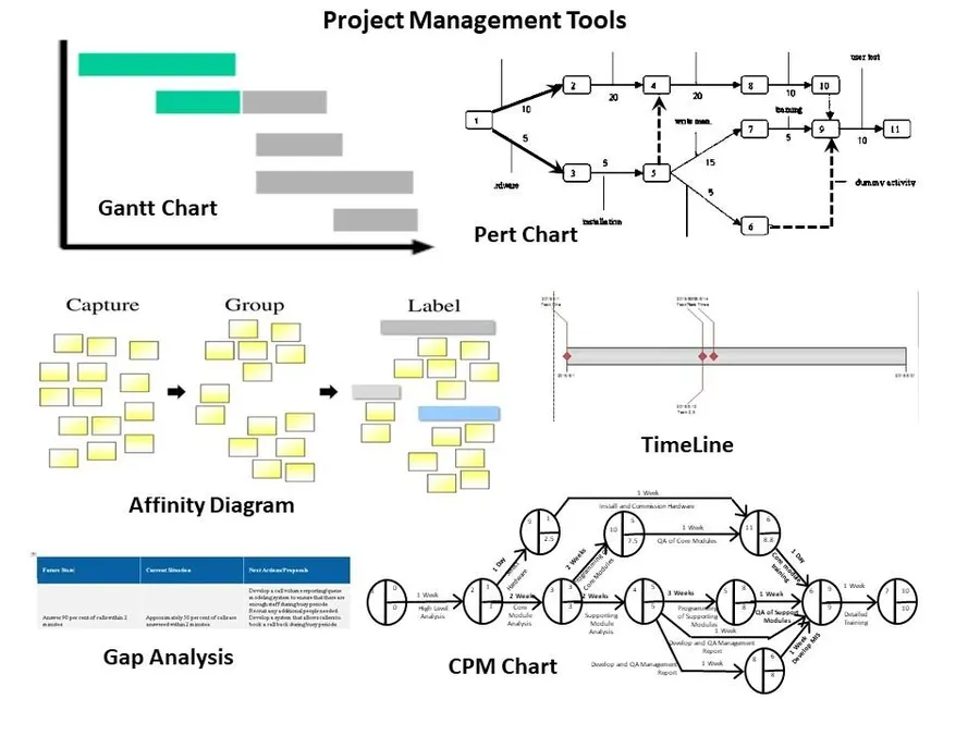
Efficient turnaround times and robust project management are paramount when selecting a PCB layout company. These factors directly impact project timelines and overall success. Understanding a company's processes for design, revisions, and communication is essential to ensure your project stays on track and within budget.
- Typical Turnaround Times
Inquire about the typical time required for initial PCB layout design and subsequent revisions. This will provide a baseline for your project planning and scheduling. - Project Management Process
A clearly defined project management process is a sign of a professional and reliable PCB layout company. Understanding their workflow can help anticipate and avoid any delays. - Communication Protocols
Effective communication channels and response times are critical for seamless collaboration. Determine who your point of contact will be and how frequently they will update you on project progress. - Revision Handling
Understand their revision process, which should be flexible and efficient to address design changes while minimizing project delays. An efficient revision process includes a clear understanding of how feedback will be incorporated and tested.
Cost-Effective PCB Layout Solutions
While cost is a crucial consideration when selecting a PCB layout company, focusing solely on the lowest price can be detrimental. The most cost-effective solution balances price with the value delivered, including design quality, manufacturability, and long-term reliability. An experienced PCB layout company will be able to optimize costs through intelligent design choices, efficient material usage, and minimizing manufacturing complications.
- Strategic Material Selection
Choosing the right materials for your PCB can significantly impact cost. Experienced companies can advise on material options that meet your technical requirements while minimizing expenses, which includes balancing performance requirements with material costs, for example, using FR-4 for general purpose and high speed laminates for signal integrity critical designs. - Optimized Layer Stack-Up
The number of layers in a PCB directly affects its manufacturing cost. A skilled layout team can optimize the layer stack-up to reduce the number of layers required without compromising functionality, which directly impacts the cost of materials and processing. - Component Placement Efficiency
Efficient component placement minimizes routing complexity, reduces the board area, and leads to lower manufacturing costs. The utilization of techniques such as component reuse or strategic placement that minimize trace lengths will lead to material savings and a more economical design. - Design for Manufacturability (DFM)
Integrating DFM principles into the design process reduces manufacturing issues that could otherwise lead to costly rework or delays. This involves optimizing the design to align with the manufacturer's capabilities, thus preventing the board from needing costly modifications. - Proactive Design Optimization
Experienced PCB layout companies proactively identify design optimizations to reduce material usage, simplify manufacturing and improve reliability during the design process, preventing costly revisions and delays.
To effectively evaluate costs, request a detailed cost breakdown from the PCB layout company. This should include cost per layer, cost per via, design time estimates, and NRE (Non-Recurring Engineering) costs. Comparing multiple detailed quotes ensures you select a provider offering the best balance of cost and value. A transparent and detailed cost breakdown is a hallmark of a reliable and professional PCB layout company.
Frequently Asked Questions About PCB Layout Companies
Navigating the selection process for a PCB layout company can raise numerous questions. This section addresses common inquiries to provide clarity and guide informed decision-making.
- What is the best PCB layout company for my specific project?
The 'best' PCB layout company is highly dependent on your project's unique requirements. Factors such as project complexity, industry-specific standards, desired turnaround time, and budget all play crucial roles. A thorough assessment of these needs is vital before selecting a provider. - How much does a PCB layout designer or company cost?
The cost of PCB layout design varies significantly based on project complexity, design density, layer count, and the experience level of the designer or company. Simpler designs with fewer layers will naturally cost less than complex designs with high component densities and multiple layers. Geographic location of the company and their overhead can also affect pricing. Request detailed quotes from multiple vendors for an accurate cost comparison and consider the overall value of design quality as a factor in cost-effectiveness. - What does PCB mean in the context of a company?
In a company, PCB refers to the 'Printed Circuit Board,' the physical substrate upon which electronic components are mounted and interconnected using conductive traces. It is a foundational element in nearly all electronic devices, and its design is crucial to the product's function and reliability. A PCB layout company, therefore, specializes in designing the specific layout of a printed circuit board. - Who are PCB designers and what do they do?
PCB designers are specialized engineers or firms that focus on the physical layout and routing of electronic circuits on a PCB. Their role is critical in translating schematic diagrams into physical PCB designs, optimizing for electrical performance, manufacturability, and cost-effectiveness. Their work also includes component placement, signal routing, thermal management, and ensuring compliance with industry standards and regulations. - What are the most important factors to consider when choosing a PCB layout company?
Key considerations include the company's expertise with your industry, their proficiency in using appropriate design tools, their ability to offer DFM analysis, turnaround time, communication and project management practices, cost, and client references. It's crucial to prioritize companies that align with the unique needs of your project. - What is DFM in PCB design, and why is it important?
DFM, or Design for Manufacturing, is the process of optimizing a PCB design to ensure that it can be manufactured efficiently and cost-effectively. A strong DFM analysis helps identify and correct potential issues early in the design process, reducing costly production delays and revisions. Aspects include considerations such as trace width, spacing, via placement, and component footprints. - What is the impact of PCB design on the performance of my electronic product?
The PCB design has a profound impact on the performance, reliability, and longevity of an electronic product. A well-designed PCB will ensure correct signal integrity, minimize noise interference, and effectively dissipate heat, all critical for product functionality. Conversely, a poorly designed PCB can lead to product malfunction and decreased longevity, requiring costly repairs or redesigns.
Comparative Analysis of PCB Layout Companies
Selecting the right PCB layout company is crucial for project success. A comparative analysis helps to navigate the numerous options available and identify a partner that aligns with your specific needs. This section provides a structured approach to evaluate and compare potential companies, emphasizing critical factors such as service offerings, industry experience, cost, and turnaround time.
| Company | Services Offered | Industries Served | Cost (Relative) | Turnaround Time (Relative) | DFM Capabilities | Communication |
|---|---|---|---|---|---|---|
| Company A | Schematic capture, PCB layout, DFM analysis | Consumer electronics, Industrial control | Medium | Medium | Strong | Good |
| Company B | PCB layout, Signal integrity analysis, Component selection | Aerospace, Medical devices | High | Long | Excellent | Excellent |
| Company C | PCB layout, DFM analysis, Prototyping | Automotive, Telecommunications | Low | Short | Basic | Medium |
| Company D | Schematic capture, PCB layout, High-speed design | High-performance computing, Data centers | High | Medium | Strong | Good |
| Company E | PCB layout, RF design, Manufacturing support | Wireless communications, IoT | Medium | Medium | Medium | Good |
This table provides a simplified comparison to guide your selection process. It is important to conduct detailed due diligence on your top choices, including checking references and assessing their capabilities in relation to your project requirements. Remember to prioritize companies that demonstrate strong communication, robust DFM capabilities, and a track record in your specific industry.
Choosing the right pcb layout company is crucial for the success of your electronic project. A careful evaluation of the company’s expertise, services, and communication ensures you receive top-quality PCB designs. Remember to clarify the project needs, examine their design tools, verify their industry experience, look for thorough DFM analysis, ensure reasonable project management, and always consider the overall value rather than solely focusing on cost. By keeping these points in mind, you’re set to work with a pcb layout company that will elevate your project from conception to reality, and bring it to market successfully.