Design PCBs Online with the Best Free Layout Makers
In today's fast-paced world of electronics, the ability to design Printed Circuit Boards (PCBs) quickly and efficiently is crucial. Just as architects use Computer-Aided Design (CAD) software to bring buildings to life, electrical engineers and hobbyists rely on PCB design tools. Thankfully, the days of expensive, standalone software are fading, giving way to powerful, free online pcb layout maker platforms that let you bring your ideas to life. This article explores top online solutions, guiding you through key features, benefits and choices to streamline your PCB design process, and transform your vision to reality.
Top Free Online PCB Layout Makers: An Overview
The advent of online PCB layout makers has revolutionized electronics design, allowing engineers and hobbyists alike to create intricate circuit boards directly within a web browser. These platforms eliminate the need for dedicated software installations, enabling collaborative design and rapid prototyping. This section introduces the leading free online options, focusing on their user interface, ease of use, and core functionalities, setting the stage for a detailed exploration of individual tools in subsequent sections.
- Key Advantages of Online PCB Layout Makers
Accessibility from any device with a web browser, elimination of software installation hassles, and built-in collaboration features. - Core Functionalities
Schematic capture, PCB layout, component library management, and output file generation (Gerber, etc.) - User Interface and Ease of Use
Intuitive drag-and-drop interfaces, integrated component libraries, and user-friendly tutorials. Ease of use is crucial, given the target audience's diverse skill levels.
EasyEDA: A Comprehensive Online Solution
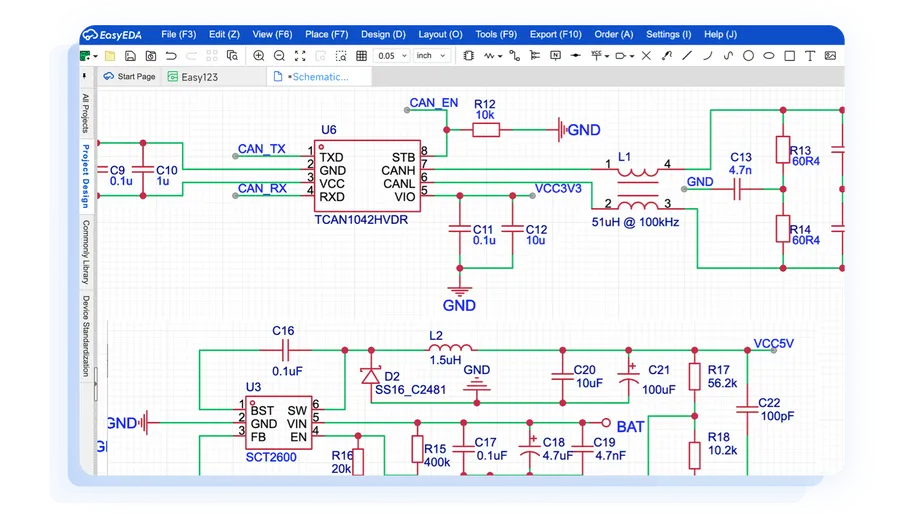
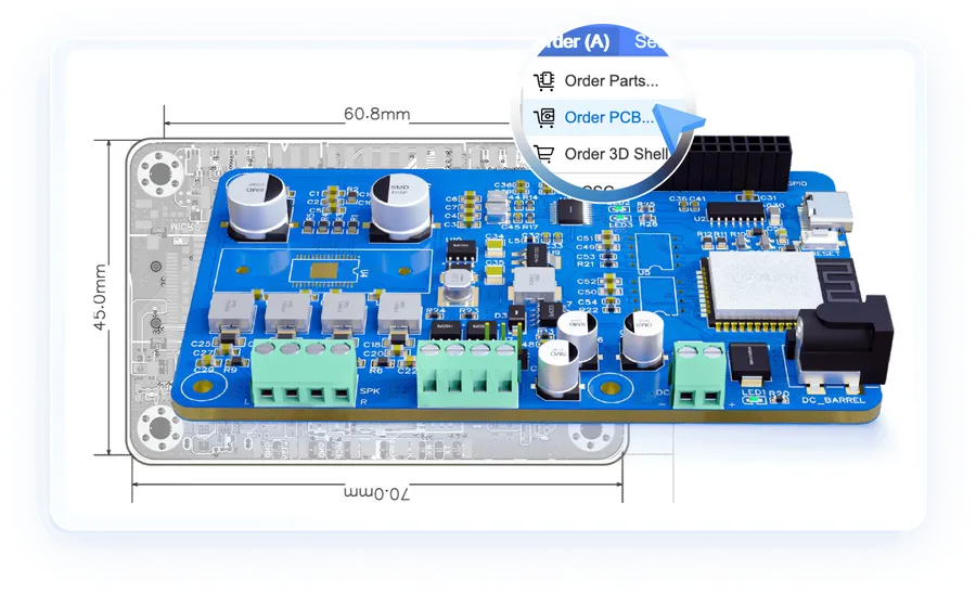
EasyEDA stands out as a robust online PCB design platform, integrating a comprehensive suite of tools that streamlines the entire design process from schematic capture to PCB layout and fabrication. Its browser-based interface facilitates accessibility and collaborative design, eliminating the need for local software installations.
- Integrated Circuit Simulator
EasyEDA includes a built-in circuit simulator, allowing designers to test and verify circuit behavior before physical implementation. This tool helps identify potential issues early in the design process, reducing costly iterations. - Extensive Component Library
A vast component library, regularly updated, provides designers with a wide selection of electronic parts. This feature simplifies the component selection process, speeding up the design phase. Users can easily find and add components to their projects, reducing manual part creation. - Direct Ordering and Fabrication Options
EasyEDA integrates seamlessly with PCB fabrication services, allowing users to order their manufactured boards directly from within the platform. This simplifies the prototyping process and eliminates the need to switch between different software and service providers. - Collaborative Design Environment
The online platform supports real-time collaborative design, enabling multiple team members to work on the same project concurrently. This is especially useful for larger teams or projects requiring contributions from different specialists.
| Feature | Description |
|---|---|
| Interface | Browser-based, accessible from any device with an internet connection. |
| Simulator | Integrated SPICE simulator for circuit verification. |
| Library | Extensive component library with regular updates. |
| Ordering | Direct PCB fabrication ordering integrated into platform. |
| Collaboration | Supports real-time collaborative design by teams. |
CircuitMaker: Altium's Free Offering for the Community
CircuitMaker, provided by Altium, distinguishes itself as a free, community-driven PCB design tool tailored for open-source hardware projects. It offers a powerful subset of Altium's professional design capabilities, enabling users to create complex circuit boards without the financial commitment often associated with high-end software.
Its strength lies in its collaborative design environment, which fosters sharing and reuse of designs within the community, providing both support and inspiration to its users.
- Key Features
CircuitMaker includes a comprehensive schematic capture tool, a PCB layout editor, and a 3D visualization tool for a complete design experience. - Community-Driven Approach
The software is built around a community platform, allowing users to easily share their work, collaborate on projects, and access a library of community-created components and designs. - Advanced Features
CircuitMaker offers advanced routing, multi-layer board support, and powerful design rule checks that allow designers to handle complex projects - Cloud-based
Being a cloud-based tool it provides a level of accessibility and ease of collaboration not found in traditional desktop software. Projects can be accessed anywhere with internet.
| Feature | Description |
|---|---|
| Free for open-source hardware | Completely free for the design of open source hardware projects. No license fees or hidden costs. |
| Schematic Capture | Allows you to create and edit electronic circuit diagrams. Provides a wide variety of tools and options for creating professional schematics. |
| PCB Layout Editor | Allows you to design the layout of a PCB. Includes powerful routing tools, layers options, and design rule checking capabilities. |
| 3D PCB Visualization | Enables visualization of your PCB design in 3D. A valuable tool for catching design flaws early and for presentations. |
| Community Platform | Provides an online platform for sharing, collaboration, and a library of components, and allows for community input. |
| Cloud-Based | Allows users to access their projects from any computer, anywhere with internet access. |
LibrePCB: The Open-Source Alternative
LibrePCB stands out as a free and open-source Printed Circuit Board (PCB) design suite, providing a viable alternative to commercial software. This cross-platform tool is designed for collaborative use, fostering a community-driven approach to electronics design. It offers comprehensive features for schematic capture, PCB layout, and component management, all within a single unified environment.
- Cross-Platform Compatibility
LibrePCB operates seamlessly across various operating systems, including Windows, macOS, and Linux. This eliminates platform-specific barriers to design, allowing collaborators to work together regardless of their system preferences. - Collaborative Design Environment
The software is developed with a focus on collaborative efforts, providing mechanisms for team-based projects. This includes features for version control and project sharing to ensure synchronization across collaborators. - Open-Source Nature
As an open-source project, LibrePCB benefits from community contributions, leading to transparent development, continuous improvement, and flexibility in adapting the software to specific user requirements. The source code is available for scrutiny and modification. - Unified Workflow
LibrePCB streamlines the entire design process by integrating schematic capture, PCB layout, and component management within a unified interface, removing the need to switch between multiple tools. - Focus on Standards
Adherence to established standards ensures compatibility with industry-standard file formats and manufacturing processes. This facilitates seamless transition from design to manufacturing.
PCB Design Software Comparison: Key Differences
Choosing the right online PCB design software is crucial for a smooth and efficient design process. This section provides a comparative analysis of EasyEDA, CircuitMaker, and LibrePCB, highlighting their key differences in terms of pricing, available features, user experience, and target audience.
| Feature | EasyEDA | CircuitMaker | LibrePCB |
|---|---|---|---|
| Pricing | Free (with paid options for advanced features) | Free | Free and Open Source |
| User Interface | Intuitive, browser-based | Desktop application, modern UI | Desktop application, cross-platform |
| Component Library | Extensive, user-contributed library with direct ordering integration | Large library, emphasis on Altium components | Growing library, community driven |
| Simulation | Integrated circuit simulator | Limited simulation capabilities | No built-in simulation capabilities |
| Community Support | Active community forums and tutorials | Strong community support, tied to Altium | Growing community, open source contributors |
| Target Audience | Hobbyists, small businesses, and education | Open-source hardware designers, small teams | Open-source enthusiasts, collaborative projects |
| File Format Support | Proprietary, imports from various software | Proprietary, Altium format compatibility | Open formats, can import from other software |
Frequently Asked Questions About Online PCB Layout Makers
This section addresses common questions regarding online PCB layout tools, providing clear answers to assist users in their design process. We aim to clarify aspects like the use of AI in design, the cost implications of various platforms, and fundamental PCB layout techniques.
- Is there AI available for PCB design?
While fully automated AI-driven PCB design is not yet widely available, some tools are starting to integrate AI for tasks like component placement and autorouting. These features can assist in optimizing layouts but still require human oversight to ensure design integrity. - Is EasyEDA free to use, or does it have paid options?
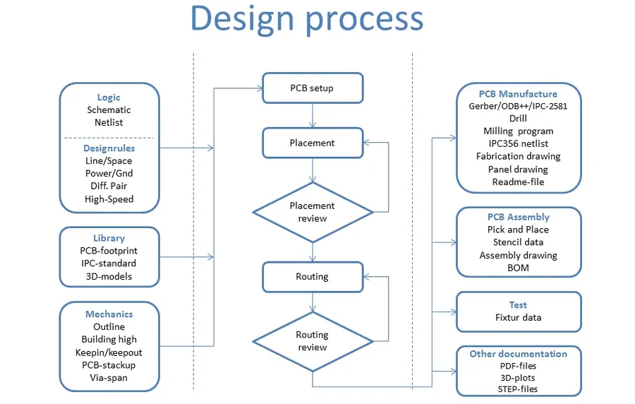
EasyEDA offers a comprehensive free tier with substantial functionality suitable for most users. It also provides optional paid services, including advanced features, professional support, and direct PCB fabrication services, which can be selected as needed. - What are the basic steps for creating a PCB layout online?
Creating a PCB layout online generally involves several key stages: importing a schematic design, arranging components, routing traces, adding vias and pads as needed, and finally generating the manufacturing files (Gerber files). Online platforms typically provide user interfaces for these steps. - Is Altium PCB design software free to use?
The full Altium Designer software is a professional-grade tool that is not free, however, Altium offers a free version called CircuitMaker. This is a community-driven platform focused on open-source hardware design. This means you will likely need to commit to a subscription if using the professional version. - Can I import existing PCB designs into online tools?
Most online PCB design platforms support importing existing design files, such as Gerber files, EAGLE files, or KiCad files. This is crucial for adapting existing designs or collaborating with other engineers and designers who may use different software. - What are the limitations of using an online PCB layout maker?
While online PCB layout tools offer convenience and accessibility, they may have limitations in terms of handling very complex designs, large numbers of layers, or very specific material requirements compared to professional desktop software. Users should assess their design needs against the tool's capabilities. - How can I ensure my PCB design is manufacturable using an online tool?
To ensure manufacturability, online PCB layout tools often provide design rule checks (DRC) which ensure the design adheres to manufacturer specifications. It is important to understand your manufacturer's guidelines and use these checks to verify your layout before sending it for fabrication.
Streamlining Your PCB Design Process
Embarking on PCB design with an online layout maker can be streamlined by focusing on structured workflows and best practices. For beginners, a methodical approach will greatly enhance efficiency and reduce errors, and for all users, leveraging these tips is the key to success.
- Start with a Clear Schematic
Before diving into the layout, ensure you have a well-defined schematic. This acts as the blueprint for your PCB. A clear schematic reduces errors and facilitates the PCB layout phase. - Component Placement Strategy
Strategically plan the placement of components, grouping related parts and considering signal flow. This helps in reducing trace lengths, minimizing noise, and optimizing the overall performance of the board. - Utilize Design Rule Checks (DRC)
Most online PCB layout makers have built in design rule checks. Use these checks to ensure that the layout meets manufacturing guidelines and prevents potential fabrication issues. - Use Layers Wisely
For multilayer boards, plan ahead and consider where power, ground, and signal traces will be routed. Utilizing a well-thought-out layer arrangement will improve signal integrity and reduce electromagnetic interference. - Master the Autorouting Function
While automatic routing features can speed up the process, it’s often beneficial to manually adjust routed traces for critical signal paths to optimize signal integrity and performance. - Regularly Review and Validate Your Layout
Before finalizing the design, check the PCB for any errors. Reviewing each element ensures that all connections are correct, trace widths are appropriate, and all design rule requirements are met, before ordering PCB fabrication. - Keep It Simple, Start Small
If you're new to PCB design, begin with a simple project. This way, you'll learn the process without facing the complexities of a complex board from the start. As you progress you can scale to more complex designs.
Ordering and Fabrication
Once your PCB design is finalized using an online layout maker, the next crucial step is ordering and fabrication. This process involves generating the necessary manufacturing files (Gerber files), selecting a suitable manufacturer, and placing your order. The quality and cost of the final product depend heavily on the chosen fabrication platform and their processes.
Many online PCB layout makers offer integrated ordering services, streamlining the transition from design to production. These platforms typically provide a selection of PCB manufacturers, allowing you to compare pricing, lead times, and manufacturing capabilities directly within the design environment. However, it is essential to carefully evaluate these integrated options.
- Integrated Ordering vs. Independent Manufacturers
Integrated ordering can be convenient, providing a seamless workflow but often with limited manufacturer choices and potentially higher prices. Using independent manufacturers allows for more customization, comparison shopping and often better pricing, but may require manual uploading of Gerber files. - Key Considerations When Choosing a Manufacturer
Factors to evaluate include the manufacturer's experience with specific PCB types, tolerances they can achieve, the materials they use, and their production capacity, additionally you should verify their quality control processes and delivery guarantees. - File Preparation
Ensure all Gerber files are generated correctly and match the design specifications. This includes layer files, drill files, and any necessary fabrication notes. Double-check all files before submitting to avoid production errors and delays.
| Factor | Integrated Ordering | Independent Manufacturer |
|---|---|---|
| Convenience | High | Low |
| Choice of Manufacturer | Limited | Wide |
| Cost | Potentially Higher | Potentially Lower |
| Lead Time | Variable | Variable |
| Flexibility | Low | High |
Advanced Features and Customization
Online PCB layout makers have evolved beyond basic single-layer designs, now offering advanced capabilities to meet the demands of complex electronic projects. These include features like multilayer support, sophisticated autorouting algorithms, and unique customization options, while limitations in handling extremely high density designs, and the scalability to work on extremely large and complex designs should also be considered.
- Multilayer Design
Designing multilayer PCBs is now standard, allowing for increased circuit density and complexity in a compact space. Most advanced online tools support multiple layers, crucial for complex routing and high-density components. - Autorouting
Autorouting simplifies the layout process by automatically routing traces based on predefined design rules. This feature drastically reduces design time, although manual routing may be necessary for critical or highly specific areas of the board. The algorithm used is often an important factor when selecting between tools. - Customization Options
Online PCB layout tools provide customization features that allow you to tailor the design to specific application needs. This may involve adjusting trace widths, custom pad shapes, and creating unique component footprints, and adjusting design rules for different aspects of the PCB layout. - Scalability and Limitations
While very useful these tools do have limitations regarding the complexity of the designs they can handle, and the scalability of these solutions for working on very large, and complicated designs is also limited, for very complex, high density, or large format designs, dedicated desktop software is still a more optimal solution.
The world of online pcb layout maker platforms has democratized the design process. With free options like EasyEDA, CircuitMaker, and LibrePCB, both beginners and seasoned professionals can bring their electronic designs to life directly through the browser. The convenience and power of these tools are constantly evolving. Now you can start designing your next great circuit today. As we look to the future, expect online PCB design platforms to become even more intuitive, collaborative, and indispensable in the electronics industry.