AnyPCBA PCB and PCBA case studies


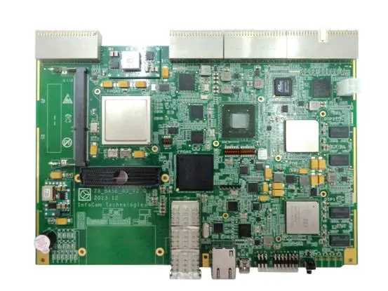
Our client, a developer of next-generation communication systems, needed a high-density PCB layout design for a complex communication board. The project presented extreme technical challenges: over 60,000 pins in a severely constrained placement area, multiple high-speed interfaces, and an aggressive two-month schedule from design to fabrication.
Key Design Challenges:
Extreme Pin Density: More than 60,000 pins on a single board with extremely limited placement space
High-Speed Interfaces: Multiple interface types including SFP+, Interlaken, QPI, PCIE3, DDR4, and DDR3
High Data Rates: Signals up to 12.5Gbps (Interlaken), 9.6Gbps (QPI), and 8Gbps (PCIE3)
Complex Power Distribution: Multiple low-voltage, high-current power supplies requiring careful power integrity planning
Aggressive Schedule: Two-month timeline requiring parallel engineering — layout and simulation work began while schematics were still under review
Stringent Standards: Required compliance with SFF8431, QPI3.0, PCIE3.0, JESD79-4, JESD79-3E
AnyPCBA provided comprehensive PCB layout design and signal integrity simulation services, working in parallel with the schematic design team to compress the project timeline.
Our design approach included:
Parallel Engineering Model: Began layout and simulation work while schematics were still under review — compressing the overall design cycle to meet the two-month deadline
Material Selection: Adopted low dielectric constant material (TU872SLK-sp) to minimize signal loss at high frequencies
High-Speed Signal Optimization: Implemented back-drill design for high-speed signal vias to reduce stub effects and improve signal quality
Comprehensive Signal Integrity Simulation: Performed SI simulation to optimize routing layers, impedance control, and signal quality across all high-speed interfaces
Power Integrity Planning: Made overall placement for power channels to ensure sufficient power plane area for high-current power supplies
Routing Strategy: Developed a comprehensive routing plan for the 60,000-pin, high-density design
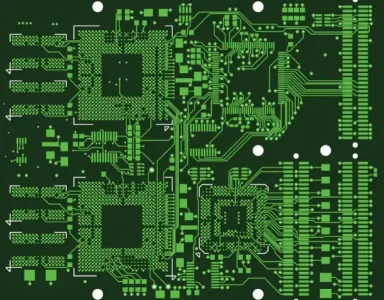
| Parameter | Specification |
|---|---|
| Total Pins | 60,000+ |
| Product Type | Communication Board |
| Key Interfaces | SFP+, Interlaken, QPI, PCIE3, DDR4, DDR3 |
| Key Standards | SFF8431, QPI3.0, PCIE3.0, JESD79-4, JESD79-3E |
| Max Signal Rate | Interlaken: 12.5Gbps / 10.3125Gbps |
| QPI: 9.6Gbps | |
| PCIE3.0: 8Gbps | |
| DDR4: 2133Mbps | |
| PCIE2.0/DMI: 5Gbps | |
| DDR3: 1600Gbps | |
| Serdes: 10.3125Gbps | |
| Material | TU872SLK-sp (low Dk) |
| Special Techniques | Back-drill, impedance control, power integrity planning |
| Project Timeline | 2 months (design to fabrication) |
On-Time Delivery: Completed the complex layout and simulation within the aggressive two-month schedule
Parallel Engineering Success: Demonstrated capability to work concurrently with schematic design — reducing overall project timeline
Signal Integrity Verified: Comprehensive SI simulation confirmed signal quality met all interface specifications
Power Integrity Assured: Careful power channel planning ensured stable power delivery for low-voltage, high-current supplies
High-Density Routing: Successfully routed 60,000+ pins in a constrained placement area
First-Pass Success: Design met all client requirements, eliminating costly re-spins
This case demonstrates AnyPCBA's capability to handle the most demanding PCB layout design challenges:
✅ Extreme pin density routing (60,000+ pins)
✅ Multiple high-speed interfaces (12.5Gbps+ signals)
✅ Advanced simulation (Signal integrity, power integrity)
✅ Parallel engineering (Compress project timelines)
✅ Complex power distribution (Low-voltage, high-current)
✅ Standards compliance (PCIe, DDR, QPI, Interlaken)
Ready to discuss your complex PCB layout design project? Contact us to learn how AnyPCBA can support your design and manufacturing needs.