AnyPCBA PCB and PCBA case studies


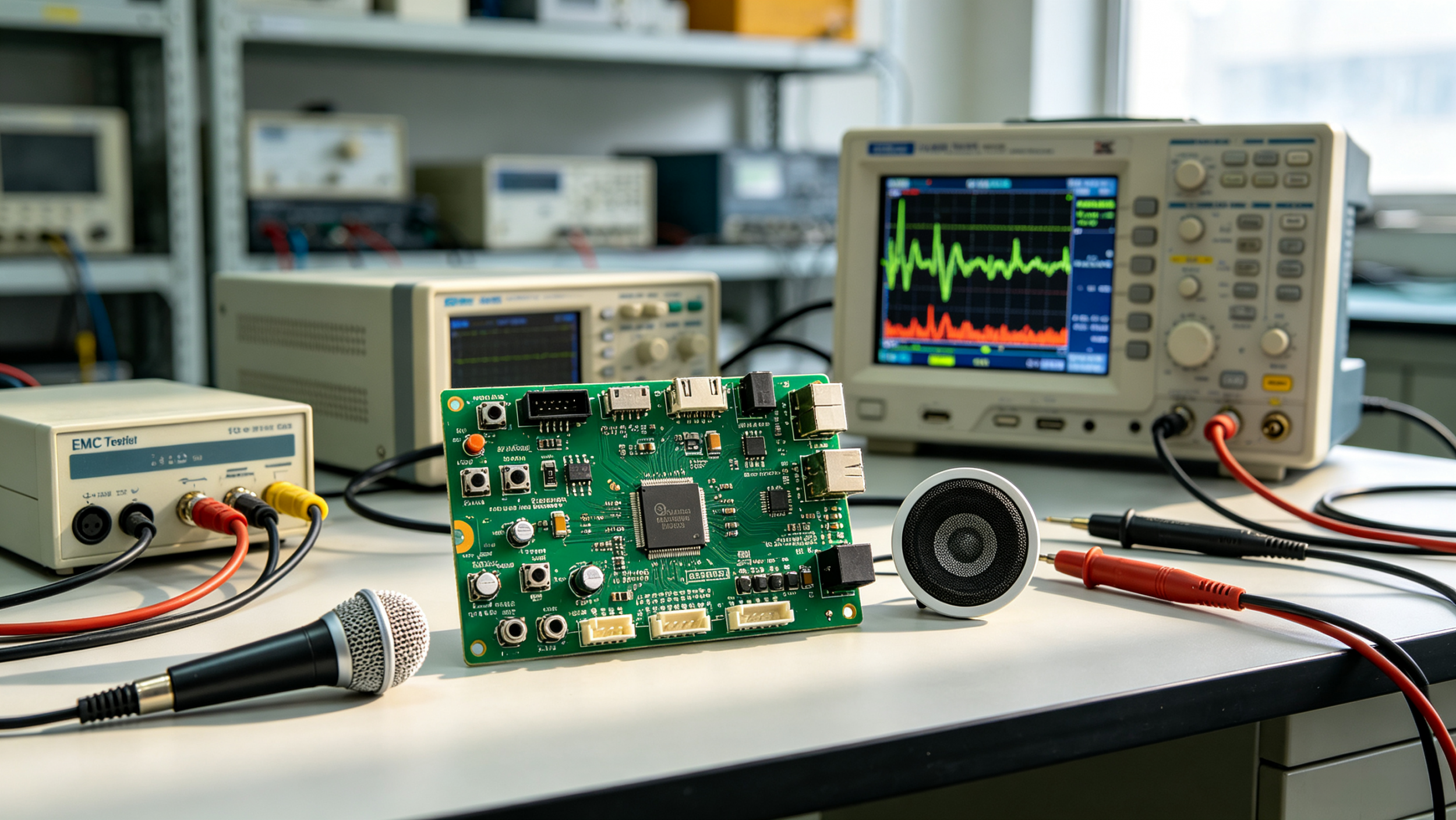
A smart home appliance brand encountered severe EMC issues during the development of their next-generation voice control panel. The product integrated a high-performance audio voice chip with microphone pickup, voice recognition, and speaker amplification. However, during FCC pre-compliance testing, radiated emissions exceeded the limit by more than 12dB, preventing the project from moving into mass production.
The core challenge the client faced was: how to balance high-fidelity audio performance with stringent electromagnetic compatibility standards within limited board space?
AnyPCBA's hardware design team conducted a comprehensive review and redesign of the client's PCB layout, focusing on 5 critical dimensions of EMC design for audio voice chips.
In the original design, digital circuits, analog audio circuits, and power circuits were mixed together, causing severe signal crosstalk.
Optimization Approach:
Analog Audio Zone: Concentrated placement of audio I/O and analog circuitry, providing a "quiet" ground plane. Traces were widened to 15mil with full guard trace routing.
Digital Control Zone: Concentrated placement of noise sources such as MCU, digital audio interfaces, and crystals. Separate digital ground return path with single-point connection through ferrite beads to analog ground.
Power Zone: DC-DC power circuits placed separately, ensuring adequate spacing between power traces and audio lines with no parallel routing.
Result: Through partition layout, interference sources and sensitive circuits were physically isolated, laying the foundation for successful EMC testing.
The original design mixed analog ground (AGND) and digital ground (DGND), allowing digital noise to inject into the analog loop through common ground impedance, resulting in audible "hiss" at the audio output.
Optimization Approach:
Physically separated AGND and DGND, with single-point connection at the main filter capacitor negative terminal through a 0Ω resistor
Adjacent layer to audio signals set as solid ground plane, providing a "clean" reference environment
For ESD protection devices and guard traces on audio interfaces, ground vias placed every 300mil
Result: Ground loop hum and noise were significantly reduced. Audio signal-to-noise ratio improved by 15dB.
The built-in power amplifier driving speakers causes large instantaneous current fluctuations, making it a major source of EMI.
Optimization Approach:
Decoupling capacitors (0.1μF + 10μF combination) placed immediately adjacent to IC power pins, minimizing high-frequency current loop length
Analog power (AVDD) and digital power (DVDD) supplied separately with ferrite beads for high-frequency isolation
Separate power ground (PGND) for the amplifier section to prevent large currents from interfering with front-end small-signal circuits through common ground
Result: Power ripple was reduced by 60%, significantly attenuating EMI radiation from the amplifier.
Crystal oscillator circuits and I2S clock lines (MCLK, BCLK) contain rich harmonics and are major EMI radiation sources on the PCB.
Optimization Approach:
Crystal placed immediately adjacent to the main voice chip, with total trace length controlled within 10mm
Clock lines guard-traced on both sides with ground vias placed at regular intervals; crystal case grounded
22Ω damping resistor placed at the source end of clock output pins to suppress overshoot and ringing
Clock lines routed away from analog audio I/O lines with no parallel routing on the same layer
Result: High-frequency radiation from clock signals was reduced by approximately 10dB — a key improvement that enabled EMC test success.
Audio interfaces (MIC input and Speaker/HP output) are critical EMC vulnerability points, connecting external environments to sensitive internal circuits.
Microphone Input Optimization:
ESD devices placed immediately adjacent to audio interface connectors, ensuring static discharge path goes through TVS to ground rather than into the chip
Microphone signals routed as differential pairs with full guard tracing, effectively canceling common-mode interference
Mic Bias and signal lines routed away from LCD cables, DRAM, and inductor component areas
Speaker/Headphone Output Optimization:
SPKP/SPKN traces routed as matched-length coupled pairs with full guard tracing; trace width calculated based on peak output current
For environments with stringent EMI requirements, LC filters placed close to the amplifier output pins
After systematic optimization across all 5 dimensions, the client's voice control panel successfully passed FCC/CE certification testing.
Core Results:
EMC Test Pass: Radiated emissions reduced from 12dB over limit to 6dB below limit — first-pass certification success
Audio Quality Improvement: Noise floor improved from -78dB to -93dB; voice recognition accuracy increased by 25%
Schedule Protection: Avoided costly redesign and re-spin; project moved to production as planned
Cost Control: Achieved through layout and grounding optimization — no additional hardware costs such as shielding cans
Smart speakers and voice assistants
Smart home appliances (voice control panels)
Security alarm systems
Automotive electronics
Small appliances and consumer electronics
EMC is not an "add-on" that can be fixed after the fact. It must be designed in from the start as a core quality attribute at every stage of PCB layout and routing.
Audio voice chip EMC design is essentially about balancing high-fidelity audio with strict electromagnetic compatibility standards within limited board space. Through systematic optimization across 5 dimensions — partition layout, grounding, decoupling, clock routing, and audio I/O — certification can be achieved on the first attempt without increasing hardware costs.
???? www.anypcba.com
???? If you're designing audio products and facing EMC or signal integrity challenges — let's talk about your project. We provide free DFM reviews and design recommendations.