AnyPCBA PCB and PCBA case studies


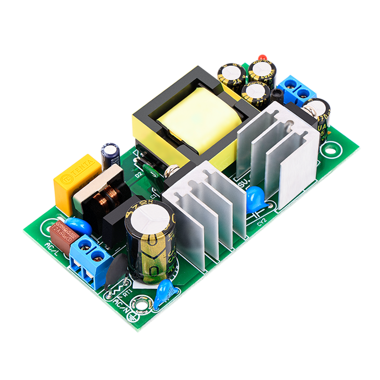
Switching power supply modules are among the most fundamental circuits in electronic systems, responsible for providing stable DC voltage conversion for other circuits on the board — from 12V to 5V, 3.3V, 1.8V, or from battery voltage up to the level required by the system. Although the topology is relatively mature, the PCB layout of a switching power supply is a critical variable that determines its performance.
A poorly laid-out Buck converter, even with the best IC and inductor, can suffer from high output ripple, excessive conducted and radiated EMI, low efficiency, and thermal hotspots. AnyPCBA has extensive experience in the design and manufacturing of power module PCBA. This case study uses a typical Buck/Boost converter as an example to systematically outline the core principles and practical considerations for switching power supply PCB layout.
Switching power supply PCB design faces multiple interconnected challenges:
| Challenge | Requirements | Design Difficulty |
|---|---|---|
| Switching Noise | Low EMI radiation, low conducted interference | High di/dt loops generate strong magnetic field radiation |
| Output Ripple | Low output voltage ripple | Improper input/output capacitor placement increases ripple |
| Conversion Efficiency | High efficiency, low loss | Parasitic inductance in power loop increases switching loss |
| Thermal Management | Good heat dissipation path | MOSFETs and inductors are primary heat sources |
| Ground Noise | Clean signal ground | Large switching currents flowing through signal ground cause noise coupling |
| Feedback Accuracy | Precise output voltage regulation | Feedback path noise interference causes regulation errors |
The physical area of the switch node (SW) must be minimized. This is the first principle of switching power supply layout.
Why? In a switching power supply, the high di/dt current loop is the primary source of EMI radiation. The larger the loop area, the stronger the radiation, and the greater the likelihood of switching noise coupling into other circuits.
Key layout points:
The connection loop between the MOSFETs, freewheeling diode/synchronous MOSFET, power inductor, and input/output filter capacitors must be extremely short and compact
Use wide copper traces or copper pours to reduce parasitic inductance and resistance
Place the input capacitor close to the MOSFET input pin, and the output capacitor close to the inductor output
Benefits of minimizing loop area:
Significantly reduces switching noise and EMI radiation
Reduces voltage spikes caused by parasitic inductance
Improves conversion efficiency
Grounding design is another critical factor determining switching power supply performance. It's essential to distinguish between power ground (PGND) and signal ground (AGND).
| Ground Type | Used In | Characteristics |
|---|---|---|
| Power Ground (PGND) | MOSFETs, inductors, input/output bulk capacitors | Carries large switching currents, high noise |
| Signal Ground (AGND) | Control IC (PWM chip), compensation network, feedback divider resistors | Carries small signal currents, sensitive to noise |
Key design principles:
Connect signal ground to power ground at a single point below the IC (typically via the PGND pin's via)
Avoid large switching currents flowing through the signal ground plane
Signal ground should remain independent and clean, connected to power ground at only one point
The trace from the output voltage sampling point to the IC feedback pin directly determines output voltage regulation accuracy.
Key design points:
Feedback traces should be short and direct, kept away from the switch node, inductor, and power traces
Use Kelvin connection when necessary, sampling directly from the output capacitor pins
Feedback divider resistors should be placed close to the IC feedback pin
Capacitor placement directly affects ripple and loop stability.
| Capacitor Type | Placement Requirement |
|---|---|
| Input Bulk Capacitor (Electrolytic) | Close to MOSFET input pin |
| Output Filter Capacitor (MLCC) | Close to inductor output |
| Output Filter Capacitor (Electrolytic/Tantalum) | Close to load |
MOSFETs and inductors are the primary heat sources in switching power supply modules.
Key design points:
Lay out large thermal pads beneath MOSFETs and inductors
Connect to inner or backside copper planes through multiple vias
Reserve space for heatsinks when necessary
For high power density designs, consider metal-core PCB or heavy copper PCB
If space permits, the following measures can further suppress EMI:
Use a ground plane to "surround" the switching power supply module
Add a magnetic shield over the inductor to suppress magnetic field radiation
Add filter circuits at input/output ports
| Outcome Dimension | Value Delivered |
|---|---|
| Conversion Efficiency | High efficiency through compact power loop and optimized grounding |
| Output Ripple | Output voltage ripple controlled within target range through proper capacitor placement |
| EMI Performance | Meets conducted and radiated standards through loop area minimization and shielding |
| Thermal Performance | Effective thermal management of MOSFETs and inductors through thermal pads and via arrays |
| System Stability | Stable regulation through clean feedback path and proper grounding strategy |
Industrial control board power conversion
Multi-rail power distribution in communication equipment
DC-DC conversion in automotive electronics
Power management modules in consumer electronics
Power subsystems for IoT devices
Low-noise power supplies for medical equipment
This project demonstrates AnyPCBA's core capabilities in switching power supply PCBA design and manufacturing:
✅ Power loop optimization — minimizing switch node area, reducing EMI radiation
✅ Grounding strategy design — power ground and signal ground separation, single-point connection
✅ Feedback path optimization — away from noise sources, Kelvin connection
✅ Thermal management — thermal pads, via arrays, heatsink reservation
✅ EMI suppression — ground plane enclosure, magnetic shielding, input/output filtering
✅ Prototype to production — supporting small-batch to medium-volume production
Need Switching Power Supply PCBA Design and Manufacturing Support?
AnyPCBA has extensive experience in power module PCBA, covering Buck/Boost converters, multi-rail power distribution, and low-noise power supplies. Our manufacturing capabilities cover 2-64 layers, including HDI, rigid-flex, heavy copper, and high-frequency hybrid processes. Our engineering team provides DFM/DFA design reviews before production to help identify potential issues in loop layout, grounding strategy, and thermal design.
Contact us to discuss your project →