
AnyPCBA PCB and PCBA case studies


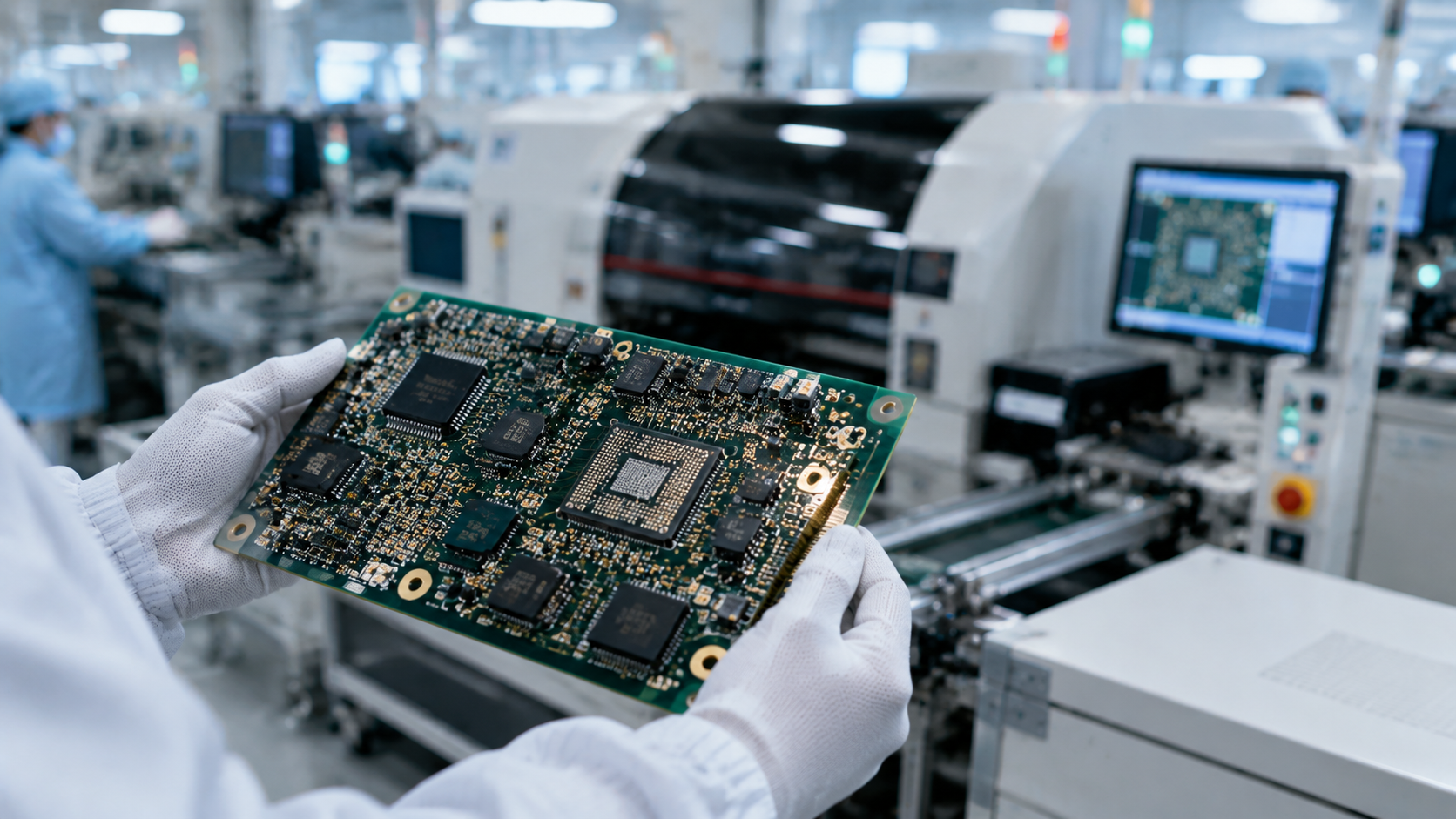
A leading new energy vehicle manufacturer faced critical challenges in their next-generation Battery Management System (BMS) design. The 12-layer control board needed to handle complex signal processing while operating in extreme environments (-40°C to 125°C). Meanwhile, a telecommunications infrastructure partner required a 16-layer hybrid PCB for 5G Massive MIMO antenna arrays operating at 28GHz.
Both projects shared common requirements: high reliability, signal integrity at high frequencies, and manufacturability at scale.
| Challenge Area | Automotive BMS | 5G Communication System |
|---|---|---|
| Signal Integrity | 25Gbps high-speed signals, impedance tolerance ±3% | 28GHz RF signal loss < 0.7dB/inch, VSWR < 1.15 |
| Thermal Management | -40°C to 125°C, 10-year service life | High power density, 128-channel array heat dissipation |
| Space Constraints | Miniaturization with 0.4mm pad pitch, HDI via technology | Complex routing, phase consistency < 2° |
| Reliability Standards | ISO 26262 ASIL-B, humidity & vibration tolerance | Long-term outdoor deployment, ESD/EMI protection |
For the automotive BMS, we selected High-Tg FR-4 (TG ≥ 170°C) with low-roughness copper foil (Rz ≤ 3μm) to ensure stable performance across the full temperature range. The 12-layer stackup was optimized for power distribution and signal integrity.
For the 5G communication system, we implemented a hybrid lamination approach combining:
Rogers RT/duroid 5880 for the 28GHz RF layers (Dk=2.2, tanδ=0.0009)
Standard FR-4 for the power and control layers
Precision thickness control (tolerance ±0.05mm) to minimize insertion loss
| Process | Specification | Result |
|---|---|---|
| Line Width/Spacing | 3/3 mil (via LDI technology) | Defect rate < 0.05% |
| Microvia Drilling | 0.05mm laser-drilled vias | Wall roughness Ra ≤ 2.5μm |
| Layer Alignment | 12-layer registration | X-Ray inspection with ±5μm precision |
| Impedance Control | 100Ω differential impedance | Tolerance within ±5% (TDR verified) |
| Surface Finish | ENIG (Au 0.05μm, Ni 5μm) | Passed 125°C high-temperature life test |
Thermal management: Embedded thermal vias and copper-filled microvias for efficient heat dissipation
Signal integrity: Full-wave simulation (HFSS) for critical RF paths, back-drilling of high-speed vias
Testability: Dedicated test points on a 100-mil grid for automated ICT, 95% test coverage
Panelization: Optimized array design for 5-5000 piece production runs
All boards underwent comprehensive testing beyond standard IPC requirements:
Environmental stress screening: Thermal cycling (-40°C ↔ 125°C, 500 cycles)
Humidity testing: 85°C / 85% RH for 1000 hours
HALT: Vibration and thermal stress to identify failure modes
AOI and X-ray inspection for BGA and hidden solder joints
Automotive BMS Board:
Signal integrity: 25Gbps signals achieved with < 1.2dB/cm loss
Thermal performance: Stable operation at 125°C with < 5% resistance drift
Reliability: Passed 1000-hour 85°C/85% RH test (insulation resistance drop < 5%)
Manufacturing yield: > 99.5% first-pass yield
5G Communication Board:
RF performance: 28GHz insertion loss reduced to 0.65dB/inch
Phase consistency: 128-channel phase error maintained within ±1.5°
Full traceability from raw materials to final test
"AnyPCBA's engineering team demonstrated deep understanding of both automotive and high-frequency design requirements. Their ability to optimize layer stackup and impedance control — combined with responsive communication from prototype to production — made them a reliable partner for our most demanding projects."
This case demonstrates AnyPCBA's capability to deliver:
Multilayer PCB fabrication from 2 to 64 layers with controlled impedance
Hybrid material processing (Rogers + FR-4, ceramic + FR-4)
Advanced technologies: HDI, blind/buried vias, back-drilling, ENIG/ENEPIG
Industry certifications: ISO 13485 (Medical) and IATF 16949 (Automotive)
Flexible production: From R&D prototyping (No MOQ) to small/medium batch
???? Ready to discuss your next high-reliability PCB project?
Contact us →


