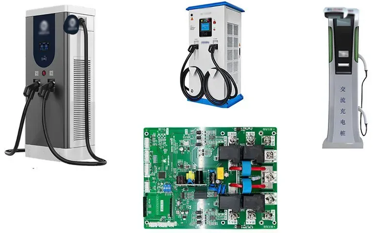
As the world increasingly shifts towards electric vehicles, the demand for efficient and reliable charging infrastructure soars. At the heart of every charging station lies a sophisticated Printed Circuit Board (PCB), orchestrating the complex dance of power delivery, communication, and safety protocols. Zero One Solution Limited, a leader in rapid prototyping and PCB solutions, stands at the forefront of this technological evolution, empowering charging station manufacturers with cutting-edge PCB solutions. This article delves into the intricacies of Charging Station Management PCB Solutions, exploring their design, functionality, and the critical role they play in ensuring a seamless and dependable charging experience.
The Critical Role of PCBs in Charging Stations
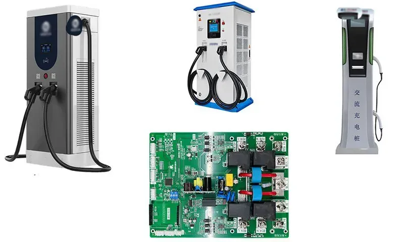
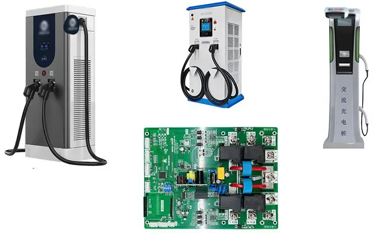
EV Charging Station PCB
Printed Circuit Boards (PCBs) are the indispensable backbone of modern EV charging stations, orchestrating the complex interplay of power conversion, communication protocols, and critical safety mechanisms. They are not merely components but the intelligent nervous system that ensures efficient, reliable, and secure power delivery to electric vehicles. The unique and demanding operational environment of charging stations, characterized by high power loads, fluctuating temperatures, and stringent safety requirements, places extraordinary demands on PCB design and manufacturing. Without robust and precisely engineered PCBs, the sophisticated functionalities expected from today's charging infrastructure would be impossible.
Power Management and Conversion PCBs are central to the efficient conversion of AC grid power to the DC power required by EV batteries, handling high currents and voltages while minimizing energy loss. This involves intricate designs for power factor correction (PFC), DC-DC converters, and switching regulators to ensure stable and clean power output, directly impacting charging speed and battery longevity. The PCB must withstand significant thermal stress generated during these high-power operations.
Communication and Data Exchange Beyond power, PCBs facilitate all communication within the charging station and with external systems. This includes communication between the charging controller and the EV (e.g., using CAN bus, PLC, or Ethernet protocols like OCPP), back-end management systems for billing and monitoring, and potentially smart grid integration. Reliable data transmission is paramount for secure authentication, status updates, and dynamic load management.
Safety and Protection Mechanisms Given the high power involved, safety is a non-negotiable aspect. PCBs integrate critical safety features such as overcurrent protection, overvoltage protection, short-circuit detection, ground fault monitoring, and temperature sensing. These mechanisms are crucial for preventing electrical hazards, protecting both the vehicle and the user, and ensuring the long-term operational integrity of the charging station itself. Fail-safe designs and redundant circuits are often incorporated into these PCBs.
Environmental and Durability Demands Charging station PCBs must be engineered to operate reliably across a wide range of environmental conditions, including extreme temperatures, humidity, dust, and potential vibrations. This necessitates the selection of high-quality materials, robust component placement, and often conformal coating to protect against moisture and contaminants. The longevity and durability of the PCB directly impact the overall lifespan and maintenance costs of the charging station.
Key Features of a Charging Station Management PCB Solution
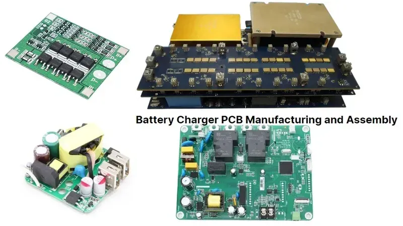
Charging Station PCB Components
A robust Charging Station Management PCB Solution is the technological backbone enabling efficient, safe, and reliable operation of EV charging infrastructure. These specialized PCBs integrate critical functionalities that govern power conversion, facilitate seamless communication, and enforce stringent safety protocols, ensuring optimal performance and longevity in demanding outdoor and industrial environments. Understanding the core features of these PCBs is paramount for developers and operators aiming to deploy next-generation charging solutions.
Advanced Power Management Charging station PCBs must efficiently handle high power loads and diverse charging protocols (e.g., AC Level 2, DC Fast Charging). Key features include robust power conversion modules (AC/DC, DC/DC), precise current and voltage regulation circuits to prevent overcharging or undercharging, and power factor correction (PFC) for grid efficiency. Integrated thermal management components, such as heat sinks and optimized trace layouts, are crucial to dissipate heat generated during high-power transfer, ensuring stable operation and extended lifespan. High-density power components are often chosen to miniaturize the PCB footprint without compromising performance, a critical consideration for sleek charging station designs.
Reliable Communication Interfaces Seamless data exchange is vital for smart charging. PCBs incorporate a variety of communication interfaces to support network connectivity (Ethernet, Wi-Fi, 4G/5G cellular modules), vehicle communication (CAN Bus, Power Line Communication (PLC) for ISO 15118), and backend management systems (OCPP - Open Charge Point Protocol). These interfaces enable real-time monitoring of charging status, remote diagnostics, user authentication, billing, and integration with smart grid systems. Robust electromagnetic compatibility (EMC) design is essential to prevent interference and ensure stable data transmission in electrically noisy environments typical of charging stations.
Feature Category
Key Functionality
Benefit for Charging Stations
Safety Mechanisms
Integrated GFCI/RCD, overcurrent/overvoltage protection, temperature sensors
Prevents electrical hazards, protects equipment and users, ensures compliance
Zero One Solution Limited: Your Partner in PCB Innovation
At the forefront of the burgeoning electric vehicle (EV) charging infrastructure, the integrity and performance of Printed Circuit Boards (PCBs) are paramount. Zero One Solution Limited, established in 2011, stands as a pivotal partner in this domain, delivering comprehensive, one-stop PCB solutions from design to rapid prototyping, manufacturing, and assembly. Our unwavering commitment to precision engineering and cutting-edge technology ensures that your charging station management PCB solutions are not just compliant, but engineered for superior reliability, efficiency, and longevity, empowering the global transition to sustainable mobility.
Rapid Prototyping Excellence Zero One Solution Limited excels in rapid-response R&D prototype manufacturing. This capability significantly accelerates product development cycles, enabling clients to quickly test, iterate, and refine their charging station PCB designs, thereby reducing time-to-market and fostering innovation at an unprecedented pace.
Comprehensive One-Stop Services We offer a seamless, integrated approach encompassing every stage of the PCB lifecycle. From initial PCB design and engineering consultation to precise manufacturing and sophisticated assembly, our end-to-end services streamline the supply chain, ensuring consistent quality and robust performance for complex charging station management systems.
Strategic Global Footprint Headquartered in Shenzhen, China, a global epicenter for electronics manufacturing, and complemented by a strategic branch office in Dubai, Zero One Solution Limited operates within a robust global PCBA supply chain network. This strategic positioning guarantees efficient access to worldwide resources, raw materials, and logistical support, ensuring timely and cost-effective delivery of high-quality PCB solutions.
Uncompromising Quality and Innovation Quality is the cornerstone of our operations. We adhere to stringent quality control standards and employ advanced testing methodologies throughout the production process to ensure every PCB meets the rigorous demands of charging station environments. Our continuous pursuit of innovation drives us to integrate the latest advancements in power electronics and communication protocols into our PCB designs.
Service Area
Key Benefit for Charging Station PCBs
Zero One Solution Limited Advantage
PCB Design
Optimized for Power & Communication
Expert engineers with deep understanding of EV charging specific requirements, including high current handling and robust data transfer protocols
Rapid Prototyping
Accelerated Development Cycle
Fast turnaround times (as low as 24 hours) for prototypes, enabling quick design validation and iteration
Manufacturing
High Reliability & Durability
Advanced manufacturing processes (e.g., IPC Class 2/3 standards) ensuring long-term operational stability in harsh conditions
Assembly
Precision & Efficiency
Automated SMT/DIP lines for high-density components, ensuring accurate placement and strong solder joints
Quality Control
Enhanced Safety & Performance
Rigorous testing (AOI, X-Ray, ICT, Function Test) to detect defects early and guarantee compliance with industry safety standards
Customization and Design Considerations for Charging Station PCBs
Custom Charging Station PCB Thermal Management
Effective charging station management hinges on highly customized Printed Circuit Board (PCB) solutions, meticulously designed to meet the unique operational demands and environmental challenges of diverse EV charging infrastructures. Generic PCBs often fall short in delivering the requisite power efficiency, communication reliability, and robust safety features necessary for high-performance charging systems, underscoring the critical need for tailored design considerations from thermal management to component selection, ensuring optimal functionality and longevity.
Thermal Management Excellence Charging stations handle significant power loads, generating substantial heat. Custom PCB designs incorporate advanced thermal management strategies, such as optimized copper pour, integrated heat sinks, and strategic component placement, to dissipate heat effectively. This prevents overheating, extends component lifespan, and maintains consistent performance, crucial for the continuous operation of charging infrastructure.
Robust Component Selection The selection of components for charging station PCBs is paramount. It involves choosing industrial-grade, automotive-qualified parts that can withstand wide temperature fluctuations, high current loads, and electromagnetic interference (EMI). This includes selecting durable connectors, high-efficiency power semiconductors (e.g., SiC/GaN), and reliable microcontrollers capable of handling complex power conversion and communication protocols.
Environmental Resiliency Outdoor and harsh indoor environments expose charging station PCBs to moisture, dust, vibration, and extreme temperatures. Custom designs integrate features like conformal coating for moisture and chemical resistance, robust enclosure interfaces, and vibration-dampening mounting solutions. This ensures the PCB's integrity and functionality are maintained under challenging operational conditions, crucial for public and commercial charging deployments.
Electromagnetic Compatibility (EMC) Design High-power switching events within charging stations can generate significant EMI, potentially disrupting communication and control signals. Custom PCB layouts prioritize EMC by incorporating proper grounding techniques, signal isolation, filtering, and impedance matching. This minimizes interference, ensuring stable data transmission for smart charging features and reliable operation of the entire system, meeting stringent international EMC standards.
Scalability and Future-Proofing A forward-looking PCB design accounts for future upgrades and scalability. This involves modular design principles, standardized interfaces, and sufficient processing headroom to accommodate new charging protocols (e.g., CCS, CHAdeMO, NACS), higher power outputs, and smart grid integration capabilities. Such foresight extends the lifespan of the charging station infrastructure and provides a competitive edge.
Rapid Prototyping: Accelerating Your Charging Station Development
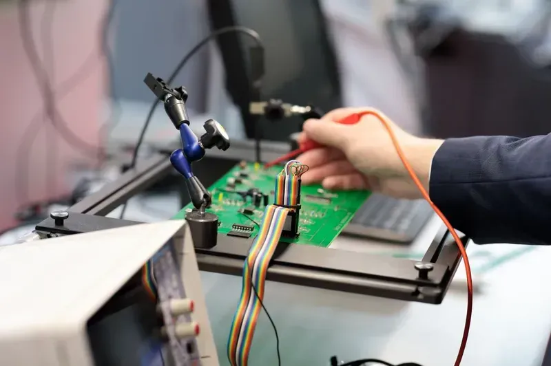
PCB Prototype Testing
In the fast-evolving landscape of Electric Vehicle (EV) charging infrastructure, the ability to rapidly iterate and validate designs is paramount. Zero One Solution Limited's rapid prototyping services are designed to significantly accelerate the development cycle of charging station PCBs, enabling manufacturers to quickly test, refine, and deploy innovative solutions. This agility is crucial for gaining a competitive edge, reducing time-to-market, and optimizing development costs by identifying and resolving potential issues early in the design phase.
Why is rapid prototyping essential for charging station PCBs? Rapid prototyping for charging station PCBs is critical because it allows for quick validation of design concepts, functionality, and performance under real-world conditions. This iterative process uncovers potential flaws in power management, communication protocols, thermal dissipation, and safety features before large-scale production, significantly reducing the risk of costly redesigns and delays.
How does Zero One Solution Limited's rapid prototyping process work? Zero One Solution Limited leverages advanced design tools and high-speed manufacturing capabilities to convert digital designs into physical PCB prototypes in record time. Our process integrates DFM (Design for Manufacturability) analysis, expedited component sourcing, and efficient assembly, ensuring that prototypes accurately reflect the final product's intended performance while maintaining high quality standards.
What benefits does rapid prototyping offer in terms of cost and time-to-market? Rapid prototyping dramatically reduces both development costs and time-to-market. By quickly identifying and correcting design flaws, it minimizes expensive retooling and material waste associated with later-stage modifications. The accelerated feedback loop allows products to reach the market faster, capitalizing on emerging opportunities and securing early market share.
Can Zero One Solution Limited accommodate specialized requirements for charging station prototypes? Absolutely. Zero One Solution Limited specializes in customized PCB solutions. Our rapid prototyping services are highly flexible and can accommodate specific requirements such as high-power handling, robust communication interfaces (e.g., CAN, Ethernet, PLC), unique form factors, and integration with advanced safety mechanisms, ensuring the prototype aligns perfectly with project specifications.
What post-prototyping support does Zero One Solution Limited provide? Beyond delivering prototypes, Zero One Solution Limited offers comprehensive post-prototyping support, including detailed performance analysis, design feedback, and recommendations for optimization. We also provide seamless transition services from prototyping to full-scale production, ensuring continuity and consistency throughout the entire product lifecycle.
Ensuring Reliability and Safety: Quality Control and Testing
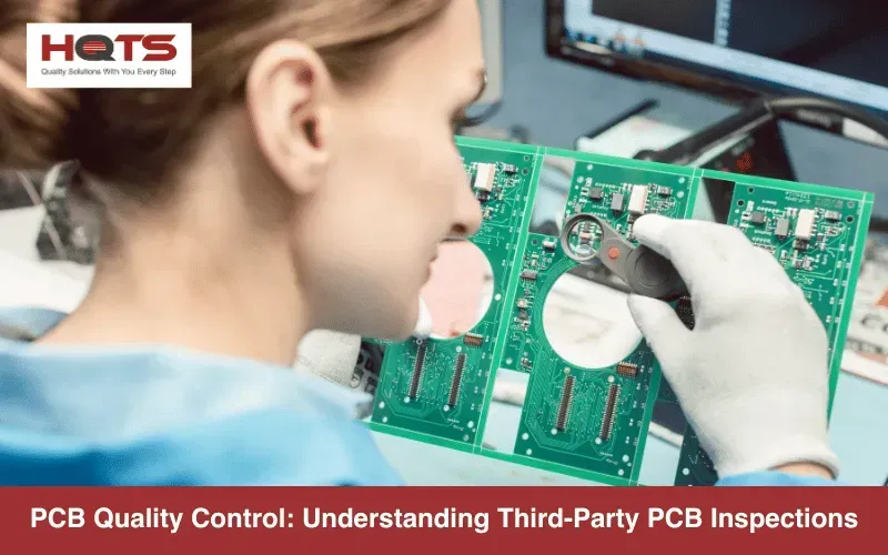
PCB Quality Control Inspection
In the demanding environment of EV charging infrastructure, the reliability and safety of a Charging Station Management PCB Solution are paramount. Zero One Solution Limited implements rigorous quality control (QC) measures and comprehensive testing procedures throughout the entire PCB lifecycle, from design verification to final product validation, guaranteeing that our solutions not only meet but exceed industry standards for performance, durability, and most critically, user safety. This meticulous approach minimizes field failures, enhances operational uptime, and protects critical investments for our clients.
Testing Phase
Key Objectives
Specific Procedures
Incoming Material Inspection (IQC)
Verify raw material quality and compliance with specifications
Visual inspection, material composition analysis (e.g., XRF), dimensional checks
In-Process Quality Control (IPQC)
Monitor manufacturing processes for defects and deviations
Automated Optical Inspection (AOI), X-ray inspection for solder joints, in-circuit testing (ICT) for component functionality and connectivity
Functional Testing
Validate the operational performance of the PCB under simulated conditions
Power delivery accuracy tests, communication protocol verification (CAN, Ethernet), load testing, thermal cycling for stress endurance
Environmental Stress Testing (EST)
Assess PCB resilience to varying environmental factors
Humidity testing, vibration testing, temperature cycling (-40°C to +85°C), salt spray testing for corrosion resistance
Reliability Testing
Predict long-term performance and identify potential failure modes
Highly Accelerated Life Testing (HALT), Highly Accelerated Stress Screening (HASS), burn-in testing to weed out early failures
Final Product Validation (FQC)
Ensure the finished PCB meets all design and performance requirements
The Future of Charging Station Technology: Trends and Innovations
The landscape of EV charging technology is rapidly evolving, driven by advancements in power electronics, communication protocols, and grid integration, all of which heavily rely on sophisticated PCB solutions. Future charging stations will be smarter, more efficient, and seamlessly integrated into broader energy ecosystems, demanding innovative PCB designs that can accommodate these emerging trends.
Wireless Charging Technology Wireless EV charging, based on inductive power transfer (IPT), is gaining traction for its convenience and reduced infrastructure footprint. This technology requires highly efficient resonant inductive coupling coils and precise control circuitry, where PCBs play a crucial role in managing power transfer efficiency, alignment detection, and safety protocols. Zero One Solution Limited is actively researching and developing high-frequency PCB laminates and optimized coil designs to support the widespread adoption of wireless charging.
Smart Grid Integration and V2G (Vehicle-to-Grid) The integration of charging stations with smart grids enables intelligent load management, demand response, and Vehicle-to-Grid (V2G) capabilities, allowing EVs to return energy to the grid. This necessitates advanced communication interfaces (e.g., PLC, Ethernet, cellular), robust power metering, and sophisticated control PCBs capable of real-time data processing and bi-directional power flow management. Our solutions focus on high-reliability PCBs that can withstand continuous power cycling and integrate diverse communication modules.
Ultra-Fast Charging and High Power Density The demand for faster charging times is driving the development of ultra-fast DC chargers (350kW and beyond). This trend places immense stress on power electronic components and PCBs, requiring superior thermal management, high current carrying capacity, and advanced materials to minimize losses. Zero One Solution Limited utilizes multi-layer PCBs with optimized copper thickness, thermal vias, and advanced substrate materials to ensure efficient heat dissipation and robust performance under extreme power loads.
Energy Storage Integration Integrating battery energy storage systems (BESS) directly into charging stations provides buffering capabilities, reducing strain on the grid and enabling off-peak charging. PCBs in these integrated systems must manage complex power conversion (AC/DC, DC/DC), battery management systems (BMS), and seamless communication between the charger, battery, and grid. We are developing compact and efficient PCB assemblies that facilitate the harmonious operation of these disparate components.
Cybersecurity and Data Privacy As charging stations become more connected and intelligent, cybersecurity becomes paramount. PCBs must incorporate hardware-level security features, secure boot mechanisms, and protected communication channels to prevent unauthorized access and data breaches. Our design philosophy includes embedding secure elements and implementing robust encryption capabilities at the PCB level to safeguard sensitive user and operational data.
Zero One Solution Limited remains at the forefront of these innovations, leveraging our rapid prototyping capabilities and extensive R&D expertise to develop future-proof PCB solutions for the evolving charging station ecosystem. Our commitment to cutting-edge technology ensures our clients are equipped to lead in this dynamic market.
Case Studies: Zero One Solution Limited's Success in Charging Station PCB Solutions
Charging station solution PCB
Zero One Solution Limited's unwavering commitment to innovation and engineering excellence is best demonstrated through our successful partnerships in the EV charging infrastructure sector. We don't just provide PCBs; we deliver comprehensive, high-performance solutions that empower our clients to overcome complex technical challenges and accelerate their market entry. Our rapid prototyping capabilities combined with meticulous quality control ensure that our contributions are robust, reliable, and future-proof, directly impacting the scalability and efficiency of charging networks globally.
Client Challenge
Zero One Solution's Approach
Solution & Impact
High-power DC fast charging (350kW+) requires advanced thermal management and robust power delivery.
Utilized multi-layer PCB design with enhanced copper pour for superior heat dissipation, coupled with high-current trace optimization.
Developed PCBs capable of sustained 350kW+ power transfer with minimal thermal stress, reducing charging times by up to 50% for compatible vehicles and extending charger lifespan.
Integration of smart grid communication protocols (OCPP 1.6J) and secure data transmission for public charging networks.
Implemented PCBs with integrated Ethernet and Wi-Fi modules, secured by hardware-level encryption and robust EMI shielding.
Enabled seamless, secure communication between chargers and central management systems, improving network stability by 30% and enabling advanced billing and monitoring features.
Development of a compact, cost-effective AC Level 2 charger for residential and commercial applications, requiring optimized component density.
Employed high-density interconnect (HDI) PCBs and strategic component placement to minimize board size while maintaining performance.
Achieved a 25% reduction in PCB footprint and a 15% reduction in manufacturing costs, enabling a more compact and competitive charger design for mass market adoption.
Need for accelerated development and rapid iteration for a new bidirectional charging (V2G) prototype.
Leveraged rapid prototyping capabilities, delivering initial PCB iterations within 7 days and subsequent revisions within 3-5 days.
Significantly shortened the R&D cycle by 40%, allowing the client to quickly test and validate Vehicle-to-Grid functionalities and secure early investor funding.
FAQs About Charging Station Management PCB Solutions
Understanding the intricacies of Printed Circuit Boards (PCBs) within Electric Vehicle (EV) charging station management is crucial for efficient and reliable operation. This section addresses frequently asked questions, providing clarity on the critical role, design considerations, and performance aspects of PCBs in modern charging infrastructure, ensuring optimal functionality and safety.
What are the primary functions of a PCB in an EV charging station? PCBs in EV charging stations primarily manage power conversion (AC to DC, or efficient DC-DC conversion), facilitate communication between the charger, EV, and central management systems, and implement critical safety protocols. They integrate power electronics, microcontrollers, and communication modules to ensure efficient energy transfer and secure data exchange.
Why is thermal management critical for Charging Station Management PCBs? Thermal management is critical because EV charging involves high power transfer, generating significant heat. Excessive heat can degrade component performance, reduce lifespan, and pose safety risks. Effective thermal management, through robust PCB design (e.g., thicker copper, thermal vias) and external cooling solutions, ensures stable operation and prevents overheating failures.
What communication protocols do Charging Station Management PCBs typically support? Charging Station Management PCBs typically support a range of communication protocols for various functions. For vehicle-to-charger communication, ISO 15118 (Plug & Charge) and OCPP (Open Charge Point Protocol) for charger-to-network communication are standard. Internally, protocols like CAN Bus, Ethernet, and RS-485 are common for component interfacing and data logging.
How does Zero One Solution Limited ensure the reliability of its Charging Station PCBs? Zero One Solution Limited ensures reliability through a multi-faceted approach, including rigorous design for manufacturability (DFM) reviews, selection of high-grade components, and advanced manufacturing processes. Comprehensive testing, including In-Circuit Testing (ICT), Functional Testing (FCT), and environmental stress screening, validates performance and durability under demanding conditions. Our commitment to ISO 9001 standards further reinforces our quality assurance.
What are the key differences between AC and DC charging station PCBs? AC charging station PCBs primarily handle power metering, communication, and control of the AC supply to the onboard charger of the EV. They are simpler as the power conversion happens within the vehicle. DC charging station PCBs are far more complex, integrating high-power rectifiers and DC-DC converters to directly supply DC power to the EV battery, requiring more advanced power electronics and robust thermal management. Zero One Solution Limited provides solutions for both, tailored to specific power levels and applications.
In conclusion, the Charging Station Management PCB Solution is the unsung hero of the electric vehicle revolution. It’s the intricate network that ensures safe, efficient, and reliable charging for the ever-growing fleet of EVs. As Zero One Solution Limited continues to innovate and refine its PCB solutions, we are committed to driving the future of EV charging, one circuit board at a time. Contact Zero One Solution Limited today to explore how our custom PCB solutions can revolutionize your charging station technology. Let's collaborate to build a sustainable future together.