In our interconnected world, printed circuit boards (PCBs) are the unsung heroes powering countless devices, from smartphones to advanced medical equipment. A 4-layer PCB is a fundamental component in many electronic designs, offering a balance of complexity and cost-effectiveness. This guide dives into the key considerations when choosing a 4 layer PCB manufacturer, helping you navigate options and understand the trade-offs between cost and quality. Whether you're designing a high-performance device or a cost-sensitive prototype, selecting the right partner is paramount to success. Let's explore what sets apart the best in the industry.
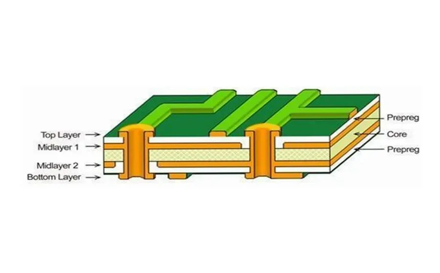
A 4-layer PCB is a printed circuit board composed of four conductive layers, typically copper, separated by insulating material. This configuration is pivotal in modern electronics, providing enhanced functionality and performance compared to simpler 2-layer boards. The layers are strategically arranged to facilitate signal routing, power distribution, and ground connections, enabling the design of more complex and reliable electronic devices.
The standard configuration of a 4-layer PCB usually includes two outer signal layers, an internal ground plane, and an internal power plane. This arrangement offers several key advantages. The dedicated ground and power planes reduce noise and signal interference, resulting in improved signal integrity. This characteristic is essential for high-speed digital circuits and sensitive analog designs. In comparison, 2-layer PCBs have significant limitations in managing these factors.
The adoption of 4-layer PCBs is driven by the need for more complex circuit designs that can't be achieved on 2-layer boards. This includes the ability to route more signals in a smaller area, the capacity to handle a wider range of voltages and currents, and the superior thermal management capabilities inherent in the design. These advantages make 4-layer PCBs suitable for a wide variety of applications, including but not limited to consumer electronics, industrial equipment, automotive systems, and communication devices.
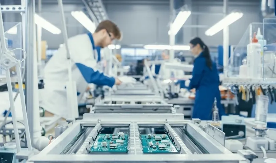
Selecting the right 4-layer PCB manufacturer is critical for ensuring the success of your electronic project. This section details the essential criteria, including manufacturing capabilities, material options, quality control processes, turnaround time, and pricing, with a specific focus on high-Tg materials often used by leading manufacturers. A careful evaluation of these factors will directly impact the performance, reliability, and cost-effectiveness of your final product.
| Factor | Description | Importance |
|---|---|---|
| Manufacturing Capabilities | Assessment of the manufacturer's equipment, technology, and capacity for handling the complexity of a 4-layer PCB design, including trace widths, spacing, and via requirements. | Ensures the manufacturer can produce PCBs to your exact specifications. |
| Material Options | Availability of various materials (e.g., FR-4, high-Tg FR-4, Rogers) and their associated performance characteristics (dielectric constant, loss tangent, etc.) | Crucial for signal integrity, thermal performance, and overall PCB reliability. |
| Quality Control Processes | Rigorous testing procedures, certifications (e.g., ISO 9001, IPC standards), and inspection methods to guarantee defect-free PCBs. | Minimizes the risk of faulty boards and production delays. |
| Turnaround Time | The time it takes from order placement to receiving the finished PCBs, considering prototyping and mass production timelines. | Critical for adhering to project schedules and meeting deadlines. |
| Pricing | The cost structure of the PCB, including setup fees, per-unit costs, and any potential discounts. | Directly impacts the overall budget of the project. |
| High-Tg Materials | Availability and experience in processing high glass transition temperature (Tg) materials, essential for applications involving high temperatures. | Crucial for reliability in demanding environments. |
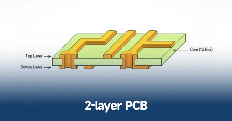
The cost of a printed circuit board (PCB) is a critical consideration in electronic design and manufacturing. A significant cost driver is the number of layers; consequently, there exists a notable cost difference between 2-layer and 4-layer PCBs, which stems from the added complexity and materials required for the latter.
| Factor | 2-Layer PCB | 4-Layer PCB |
|---|---|---|
| Material Cost | Lower | Higher (due to additional layers and prepreg material) |
| Manufacturing Complexity | Lower | Higher (more complex etching, lamination, and registration processes) |
| Manufacturing Time | Shorter | Longer(additional processes) |
| Fabrication Cost | Lower | Higher (due to material and process costs) |
| Design Flexibility | Limited | Higher (more routing space, better signal integrity) |
| Typical Applications | Simple electronics, basic circuits | More complex circuits, high-speed applications, impedance control required |
Several factors contribute to cost variations within 4-layer PCB manufacturing. These include:
Furthermore, the cost difference between prototyping and mass production for a 4-layer PCB is substantial. Prototypes often require customized setups and smaller batch runs, leading to higher per-unit costs. Mass production benefits from standardized processes and economies of scale, which lowers the cost per board considerably. Therefore, early design optimization to reduce complexity can significantly reduce the cost of mass production.
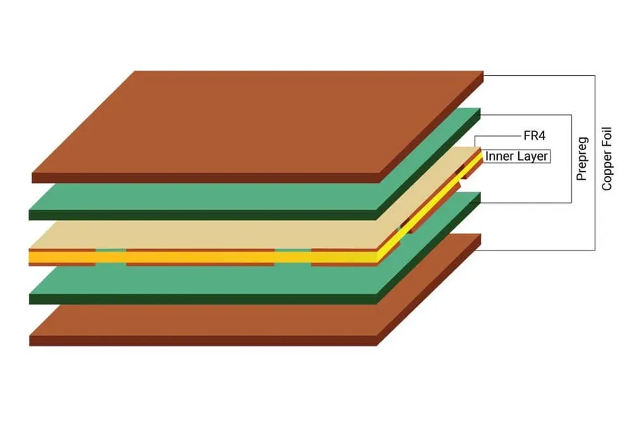
The selection of materials for a 4-layer PCB is paramount, directly influencing its performance, reliability, and cost. The most common material is FR-4, a glass-reinforced epoxy laminate, offering a good balance of electrical properties, mechanical strength, and cost-effectiveness. However, specialized applications may require alternative high-performance materials.
| Material | Description | Dielectric Constant (εr) | Loss Tangent (tan δ) | Typical Applications |
|---|---|---|---|---|
| FR-4 | Standard glass-reinforced epoxy laminate. Cost-effective and widely used. | 4.3 - 4.8 | 0.02 - 0.03 | General purpose PCBs, most electronic devices. |
| High-Tg FR-4 | FR-4 with a higher glass transition temperature (Tg). Improves performance in high-temperature environments. | 4.2-4.7 | 0.018-0.025 | Automotive electronics, industrial control systems. |
| Polyimide | High-performance polymer with excellent thermal stability and electrical properties. Suitable for flexible circuits. | 3.2-3.5 | 0.002 - 0.008 | Aerospace, medical devices, flexible electronics. |
| Rogers Materials (e.g., RO4350B) | Advanced ceramic-filled PTFE laminates. Excellent for high-frequency applications due to low loss. | 3.48 | 0.0037 | RF and microwave circuits, high-speed digital systems. |
| Teflon (PTFE) | Low dielectric constant and extremely low loss tangent. Ideal for very high-frequency applications. | 2.1 | 0.0002 | Satellite communication, radar systems. |
FR-4, with its varying Tg (glass transition temperature) options (standard, mid, and high Tg), is the most common choice for cost effective solutions. The selection of higher performance materials, such as those offered by Rogers or the use of Polyimide laminates, is dictated by specific application needs such as those involving high temperature, high frequency, or flexural requirements. Material selection should be based on the performance requirements of the final application, while carefully considering cost implications. Proper material choices will help meet the design specifications, ensure product reliability, and minimize unnecessary expenditures.
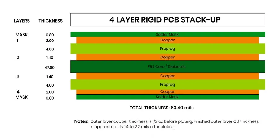
The stack-up design of a 4-layer PCB is paramount to its performance, influencing critical aspects such as impedance control, signal integrity, and thermal management. A well-planned stack-up ensures the board operates efficiently and reliably, while a poorly designed one can lead to signal degradation, noise issues, and thermal problems, ultimately affecting the overall functionality of the electronic device.
Fundamentally, a 4-layer PCB comprises four conductive layers separated by dielectric material. Typically, these layers are arranged as follows: a signal layer on the top, a ground plane, a power plane, and another signal layer on the bottom. This arrangement is not arbitrary but rather carefully considered to optimize the circuit's electrical and thermal performance. The exact spacing and thickness of each layer and the dielectric material used are all critical parameters influencing the performance of the board.
| Aspect | Impact on PCB Performance |
|---|---|
| Impedance Control | Ensures that signal reflections are minimized by matching the characteristic impedance of the traces to the impedance of other components in the circuit. |
| Signal Integrity | Proper grounding and power distribution minimizes signal noise and crosstalk and maintains the quality of the signal being transmitted by the PCB. |
| Thermal Management | Thicker copper planes efficiently dissipate heat, preventing component damage and improving overall reliability. |
A key benefit of carefully managing stack-up design is enhanced impedance control. By precisely defining the spacing between signal layers and ground or power planes, we can ensure that the signal traces on the PCB maintain a consistent characteristic impedance. This is crucial for preventing signal reflections, which can lead to signal distortion and data errors, particularly in high-speed digital circuits. For example, in high-speed communication interfaces, the impedance of signal lines should be closely matched to 50 ohms, or 75 ohms for RF applications, and that is ensured by proper stack-up design. In addition, signal integrity is significantly enhanced through effective stack-up design. By locating the ground and power layers adjacent to the signal layers, we can minimize signal crosstalk and reduce noise from external interference. The presence of these planes also acts as shields, reducing electromagnetic interference (EMI) and ensuring that the board does not generate undue EMI and impact other electronic devices.
Furthermore, a carefully designed stack-up can dramatically improve thermal management of the PCB, particularly for densely populated boards with components that dissipate a lot of heat. The copper planes, especially those in the ground and power layers, act as heat spreaders, effectively dissipating heat away from hot spots. Proper layer thicknesses and materials also contribute to effective thermal pathways, lowering operating temperatures and boosting the reliability of the overall system. Hence, the stack-up design, far from being an afterthought, is a critical element in achieving a functional, high-performance, and reliable PCB.
Selecting the right manufacturer for 4-layer PCBs requires a thorough evaluation of their capabilities, ensuring they can meet both your current and future needs. This evaluation extends beyond pricing, encompassing certifications, technological prowess, equipment, testing protocols, and special service offerings, such as those for ENIG (Electroless Nickel Immersion Gold) PCBs.
Here’s a detailed breakdown of key evaluation points:
By meticulously evaluating these aspects, you can select a 4-layer PCB manufacturer that not only meets your current production needs but also ensures the long-term success and reliability of your electronic products.
The transition from a 4-layer PCB prototype to mass production involves significant shifts in process, volume, and cost considerations. Understanding these differences is crucial for efficient and cost-effective scaling of electronic products. Prototyping focuses on validating design functionality, while mass production optimizes for volume and cost-efficiency.
| Feature | Prototyping | Mass Production |
|---|---|---|
| Volume | Low (typically a few to tens of boards) | High (hundreds to thousands or more) |
| Cost per Unit | High | Lower |
| Turnaround Time | Fast | Longer, dependent on quantity |
| Process | Flexible, may include manual steps | Automated, standardized processes |
| Design Iteration | Common, often multiple rounds | Limited, finalized design |
| Tooling and Setup | Minimal, more flexible | Significant, requiring specific tooling |
| Quality Control | Thorough but manual | Automated testing and statistical process control |
During prototyping, the focus is on rapid iteration and validating design concepts. This phase utilizes more manual processes and is less concerned with cost per unit as the main goal is to test and refine the design. Mass production, however, requires the implementation of highly efficient and automated processes to keep costs low, while maintaining high yield and quality. This is facilitated through higher investments in tooling and production setup, which amortizes over the larger volumes.
Scaling up from prototyping to mass production involves several considerations:
This section addresses common questions regarding 4-layer PCB manufacturing, providing clear, concise answers to help you understand key aspects of this technology, from layer composition to cost considerations and manufacturer selection.
Selecting the right 4-layer PCB manufacturer is crucial for ensuring the quality, reliability, and cost-effectiveness of your electronic projects. This section provides a comparative overview of several leading manufacturers, highlighting their strengths and weaknesses to help you make an informed decision.
| Manufacturer | Strengths | Weaknesses | Pricing | Customer Service | Specialization |
|---|---|---|---|---|---|
| PCBWay | Wide range of capabilities, including advanced PCB technologies; good online platform; fast turnaround times for prototypes. | Can be slightly more expensive than some competitors for high volume production. | Competitive for prototyping and small to medium-sized production runs. | Generally responsive and helpful, with online support. | Prototyping and small to medium-sized production. |
| JLCPCB | Very cost-effective for small to medium batch production; good quality for the price; automated online ordering system. | Fewer advanced technology options compared to PCBWay; longer lead times for complex designs. | Highly competitive, particularly for budget-conscious projects. | Adequate online support; may have longer response times for complex issues. | Small to medium batch production. |
| RushPCB | Known for its rapid turnaround times, particularly for urgent projects, extensive manufacturing capabilities and global presence. | Can be more expensive than other options, particularly for standard production. | Higher than average due to focus on speed and complex projects. | Provides personalized and responsive support, particularly for urgent projects. | Rapid prototyping and complex designs. |
| Advanced Circuits (AdvancedPCB) | Strong focus on high-quality and reliability; excellent customer support; specializes in complex PCBs. | Higher prices than competitors, not ideal for budget-conscious projects. | Premium pricing reflecting their focus on quality and expertise. | Excellent support with highly trained engineers available for technical assistance. | High-reliability and complex PCBs. |
Selecting the appropriate 4 layer PCB manufacturer is crucial for ensuring the quality, cost-effectiveness, and timely delivery of your electronic products. By considering factors such as material selection, manufacturing capabilities, and cost, you can make informed decisions that lead to success. A reliable 4 layer pcb manufacturer not only produces the boards but also provides valuable support throughout the design and production process, ensuring your project meets its objectives and performance goals. As the technology advances, continue to re-evaluate your manufacturing partners to stay competitive and efficient.

