Choosing the Right 6 Layer PCB Manufacturer: A Comprehensive Guide
2025.01.14
In today's rapidly evolving technological landscape, the printed circuit board (PCB) stands as an indispensable component underpinning countless electronic devices. From the complex aerospace systems to everyday smartphones, PCBs, particularly 6-layer PCBs, are the linchpin of their functionality. The selection of a dependable 6 layer PCB manufacturer directly impacts the quality and reliability of your final product. This guide will walk you through the key aspects to consider, including stackup design, manufacturing processes, cost factors, and how to identify a suitable 6 layer PCB manufacturer to bring your product from conception to reality.
Understanding 6 Layer PCBs: Structure and Applications
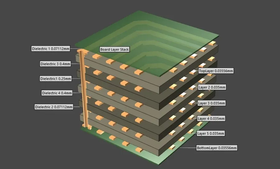
6 Layer PCB
A 6-layer PCB is a printed circuit board composed of six distinct layers of conductive material, typically copper, interleaved with insulating layers, commonly referred to as the substrate. This multi-layered structure enables complex circuit routing and provides enhanced signal integrity compared to single or double-layer boards, catering to more sophisticated electronic applications.
Layer Arrangement The typical 6-layer PCB structure includes two outer signal layers, two internal signal layers, and two power/ground planes. The precise arrangement can vary based on design requirements and intended application. The power and ground planes are strategically placed to minimize noise and provide a stable reference for signal layers.
Insulating Layers These layers are typically made from materials like FR-4, a flame-retardant fiberglass composite, which provides electrical insulation and mechanical support. Other materials with specific properties, such as higher thermal conductivity or lower dielectric constant may be used based on application-specific requirements.
Signal Layers These layers carry the electrical signals within the circuit. Proper layer planning is necessary to minimize signal coupling and interference by controlling impedances and spacing. The internal signal layers are shielded to reduce electromagnetic interference (EMI).
Power and Ground Planes These layers are dedicated to distributing power and providing a stable ground reference for the circuit. Their large surface area can act as a shield and also provide good heat dissipation.
Typical Applications 6-layer PCBs are frequently used in applications requiring higher circuit density and improved performance such as industrial control systems, telecommunications equipment, high-performance computing devices, medical instrumentation, automotive electronics, and advanced consumer electronics.
Key Considerations When Choosing a 6 Layer PCB Manufacturer
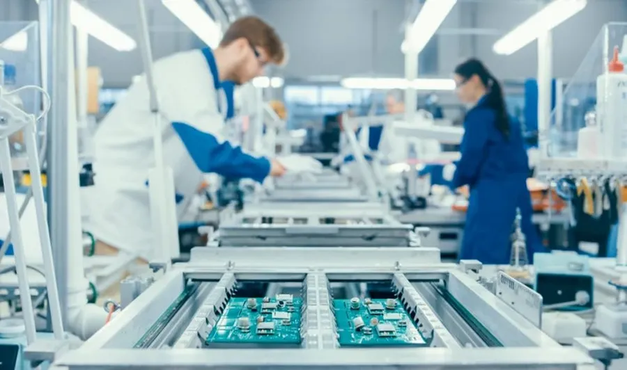
PCB Factory
Selecting the right 6-layer PCB manufacturer is paramount for ensuring the quality, reliability, and performance of your electronic products. This decision hinges on several critical factors, each requiring careful evaluation to align with your project’s specific needs and constraints.
Manufacturing Capabilities A crucial aspect is assessing the manufacturer's capacity to handle the technical complexities of 6-layer PCBs. This includes their precision in trace width and spacing, drilling capabilities (especially for microvias), and ability to manage various PCB materials. Look for manufacturers with the appropriate equipment and experience to meet your design specifications.
Experience and Expertise The manufacturer's track record in producing 6-layer PCBs is a strong indicator of their reliability. Prior experience with similar projects, along with a skilled workforce, can significantly reduce potential issues and ensure consistent quality. Consider manufacturers specializing in complex multilayer boards.
Quality Control Processes A robust quality control system is vital for preventing defects and maintaining high production standards. Manufacturers should have well-defined procedures for material inspection, in-process checks, and final product testing. This ensures that every PCB meets the required specifications and performance criteria.
Certifications and Compliance Ensure the manufacturer holds relevant industry certifications, such as ISO 9001 for quality management or IPC standards for PCB manufacturing. These certifications demonstrate a commitment to quality and compliance with recognized standards, providing an assurance of manufacturing competence.
Turnaround Time and Delivery Schedules The speed at which a manufacturer can produce and deliver your PCBs can directly impact your project timeline. Assess their typical lead times and their ability to meet your specific production deadlines. Flexibility in scheduling and communication are also important.
Cost and Pricing Structure While cost is an important factor, it shouldn't be the sole determinant. Evaluate the manufacturer's pricing structure for transparency and consider the balance between price and quality. Look for manufacturers that offer competitive pricing without compromising on material quality or production processes.
Communication and Customer Service Effective communication is key for a smooth manufacturing process. Choose a manufacturer that is responsive to inquiries, provides clear updates, and offers technical support. Reliable customer service and open communication channels are critical for addressing any issues that may arise during production.
6 Layer PCB Stackup: Design and Optimization
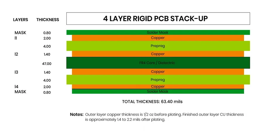
PCB Stackup
The 6-layer PCB stackup is critical for optimizing performance, ensuring signal integrity, managing impedance, and facilitating effective thermal dissipation. A well-designed stackup is not merely about layering; it's about strategically positioning the conductive and insulating materials to achieve the desired electrical and thermal characteristics.
Understanding the nuances of a 6-layer stackup is essential for high-speed digital designs and sensitive analog circuits where controlled impedance, minimal noise, and efficient heat management are paramount.
Signal Integrity Proper stackup design minimizes signal reflections, crosstalk, and electromagnetic interference (EMI), ensuring clean and reliable signal transmission. Layer assignments should prioritize sensitive signals with adequate reference planes.
Impedance Control Controlled impedance traces are essential for maintaining signal quality, especially in high-frequency applications. The geometry of the signal traces and the dielectric material of the insulating layers affects characteristic impedance, so a properly designed stack-up is necessary to achieve this control.
Thermal Management Strategic placement of power and ground planes can act as thermal conduits, facilitating heat dissipation from components and preventing localized hot spots. Proper via placement helps to ensure that the heat can effectively move to the appropriate heat dissipation layer.
Signal layers are not symmetrical around a plane but are distributed around power and ground planes.
Applications with mixed analog and digital signals, or where thermal performance is not critical.
Good power integrity due to power and ground planes. Potential for noise issues if not implemented correctly.
Can result in more noise than a symmetrical stackup due to the imbalanced stack.
The 6 Layer PCB Manufacturing Process: A Step-by-Step Guide
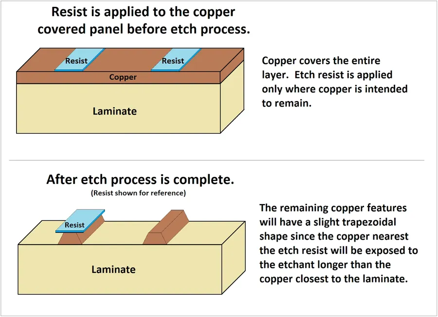
PCB Etching
The fabrication of a 6-layer PCB is a complex, multi-stage process requiring precision and stringent quality control. It begins with the design and culminates in a fully functional circuit board. Each step is crucial to ensuring the final product meets the required specifications for its intended application.
Design Review and Preparation The process starts with a thorough review of the PCB design files (typically Gerber files) to check for manufacturability, ensuring all specifications and clearances are met. This involves verifying drill sizes, track widths, spacing, and other critical parameters, followed by panelization, which arranges multiple PCB designs on a larger fabrication panel to increase manufacturing efficiency.
Inner Layer Imaging and Etching This stage focuses on the four core layers of the 6-layer PCB. The copper clad laminates are coated with a photosensitive resist, which is then exposed to UV light through a phototool that contains the circuit pattern. The exposed resist hardens, while the unexposed resist is washed away, revealing the copper to be etched. A chemical etchant removes the exposed copper, leaving behind the desired circuit pattern.
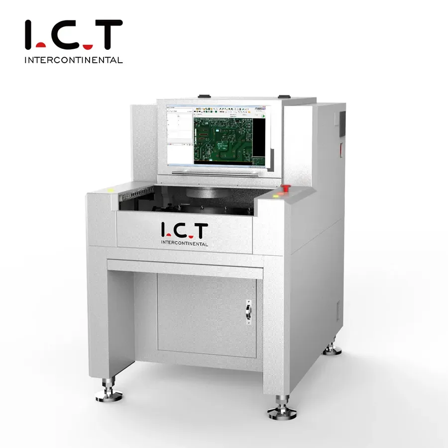
Automated Optical Inspection (AOI) for Inner Layers Before lamination, the etched inner layers undergo AOI to detect any defects, such as shorts, opens, or trace irregularities. This ensures the quality of the individual layers, preventing defects from being incorporated into the final board. Any faulty panels are removed for rework or discarding.
Lamination The core layers, along with prepreg (an insulating material with adhesive properties), are stacked in a precise sequence and placed under high pressure and temperature in a lamination press. This process bonds the layers together to create the 6-layer structure. Accurate alignment of the layers is essential for proper functionality.
Drilling After lamination, holes for vias (electrical connections between layers) and component mounting are drilled using precision Computer Numerical Control (CNC) drilling machines. These holes are often plated to provide electrical continuity and mechanical strength.
Copper Plating A thin layer of copper is applied to the surface of the board, including the inside of the drilled holes, using an electrolytic plating process. This plating ensures that the vias are conductive and also prepares the board for subsequent outer layer processing. Copper thickness must meet design specifications for current carrying capacity.
Outer Layer Imaging and Etching Similar to inner layer processing, the outer layers are coated with a photosensitive resist, exposed to UV light using a phototool, developed to remove unexposed resist, and then etched to reveal the final circuit pattern. This includes component pads, tracks, and other surface features.
Solder Mask Application The solder mask (a protective coating) is applied to the entire board except for the areas where components will be soldered. This prevents solder from flowing to unwanted areas during assembly, and also protects the copper circuitry. The solder mask is typically green, but other colors are available.
Surface Finish Various surface finishes, such as HASL (Hot Air Solder Leveling), ENIG (Electroless Nickel Immersion Gold), or OSP (Organic Solderability Preservative), are applied to the exposed copper pads. These finishes enhance solderability and protect the copper from oxidation.
Silkscreen Printing Silkscreen, usually white, is printed onto the solder mask, typically including component designators, logos, and any other necessary information. This provides assembly and debugging guidance.
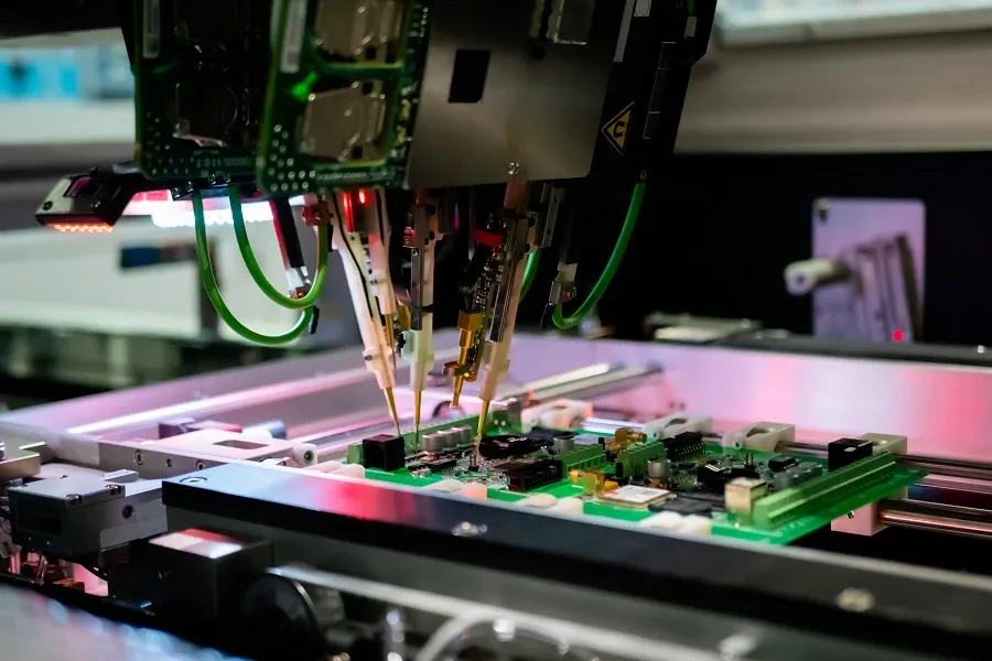
Electrical Testing The manufactured boards undergo a thorough electrical test, typically using a flying probe or bed-of-nails tester, to verify continuity and resistance according to the design specifications. This identifies any shorts, opens, or other electrical failures.
Final Inspection and Packaging After successfully passing all tests, the PCB boards are given a final visual inspection. Any defects or inconsistencies are addressed. The boards are then packaged for shipment, ensuring they are protected during transit.
Cost Factors and Pricing for 6 Layer PCBs
PCB Cost Analysis
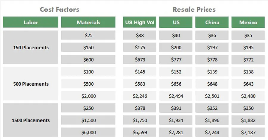
Understanding the cost drivers of 6-layer PCB manufacturing is crucial for effective budgeting and project planning. This section details the primary factors influencing the final price, enabling informed decision-making when selecting a manufacturer and managing costs.
Cost Driver
Description
Impact on Cost
Material Costs
The type and grade of materials (e.g., FR-4, Rogers) used for the core and prepreg layers.
Higher-grade materials increase cost.
Layer Count
The number of layers in the PCB design. For a 6-layer PCB, this is a fixed cost driver but affects complexity.
Directly increases with layer count
PCB Size & Dimensions
The overall surface area and physical dimensions of the circuit board.
Larger boards require more materials and processing time and increase costs
Copper Thickness
The thickness of copper on each layer.
Thicker copper layers will increase material usage and manufacturing difficulty
Hole Count & Type
The number of through-hole vias, blind vias, and buried vias. Smaller hole sizes and more complex via structures drive up costs.
Complex via structures increase costs.
Surface Finish
The type of surface finish (e.g., HASL, ENIG, immersion tin) applied.
ENIG or other high performance coatings will increase the cost
Solder Mask and Silkscreen
The cost of applying solder mask and silkscreen. Multiple colors and tight tolerances will increase the price
Additional colors and precise tolerances add to the cost.
Testing Requirements
Specific electrical and functional test procedures requested.
Rigorous testing adds to costs.
Order Volume
The total quantity of PCBs to be manufactured in each order.
Higher volumes reduce the per unit cost
Turnaround Time
The time needed for PCB manufacturing.
Express manufacturing options will increase cost.
Tooling and Setup
Initial setup costs like photo tools for each layer. These can amortized by large volume orders
One-time setup fees increase cost for low-volume orders.
Estimating the cost of a 6-layer PCB requires a thorough understanding of these variables. Requesting quotations from multiple manufacturers can give a better indication of overall cost. Consider the long-term impacts when evaluating cost. Lower material cost could mean lower board quality.
Comparing 6 Layer PCB Manufacturers: Key Differences and Features
PCB Inspection Machine
Selecting the right 6-layer PCB manufacturer is crucial for ensuring the quality, reliability, and performance of your electronic products. This section provides a comparative analysis, highlighting key differences, strengths, weaknesses, and specialization areas among various manufacturers to facilitate informed decision-making.
Manufacturer
Strengths
Weaknesses
Specialization
Typical Lead Time
Cost (relative)
Minimum Order Quantity
JLCPCB
Low cost, fast turnaround, online ordering platform
Limited advanced material options, less focus on high reliability applications
Prototyping, small to medium batch production
3-7 days
Low
1-5 pcs
PCBWay
Wide range of manufacturing capabilities, good customer support
Can be slightly more expensive than JLCPCB, lead times can vary
Prototyping, medium to large batch production, specialized technologies
5-10 days
Medium
5-10pcs
Advanced Circuits
High-quality production, strong focus on reliability, good for complex PCBs
Higher cost, longer lead times
Aerospace, military, medical, high reliability applications
7-15 days
High
Varies by project
Other Major Manufacturers
Established market presence, diverse service offerings, global reach
May have higher costs, longer lead times, variable customer support.
Large-scale mass production, wide range of industries
7-21 days
Medium to High
Varies by project
The table above provides a general comparison. It is essential to conduct a detailed evaluation based on specific project needs. Factors such as the complexity of the design, material requirements, production volume, and required testing should be considered when selecting a manufacturer.
Frequently Asked Questions about 6 Layer PCB Manufacturing
This section addresses common queries regarding 6-layer PCB manufacturing, providing concise answers to assist in understanding their applications, design considerations, and selection of suitable manufacturers.
What are typical applications for 6-layer PCBs? 6-layer PCBs are frequently utilized in applications requiring a balance between complexity, performance, and cost. They are commonly found in industrial control systems, high-end consumer electronics, communication equipment, and medical devices, where increased routing density and signal integrity are essential.
What is a recommended 6-layer PCB stack-up? A common and generally recommended 6-layer stack-up involves two signal layers on the top and bottom surfaces, two internal ground planes and two power planes. This configuration provides good signal integrity by placing signal layers adjacent to ground planes, and allows effective power distribution. The order of layers and the thickness of the core and prepreg can vary based on specific application requirements and impedance control needs.
How do I choose the right 6-layer PCB manufacturer for my specific needs? Selecting a suitable manufacturer depends on several factors including their manufacturing capabilities, certifications (ISO 9001, etc.), experience with 6-layer boards, and specific technology requirements. It is crucial to evaluate their prototyping and production turnaround times, quality control processes, and cost, as well as whether their expertise aligns with the complexity of your design.
Are 6-layer PCBs suitable for high-speed signal applications? Yes, 6-layer PCBs are well-suited for high-speed signal applications, provided they are designed with proper impedance control and signal integrity techniques. The arrangement of signal and ground planes is crucial for minimizing signal reflections and crosstalk.
What is the typical lead time for manufacturing 6-layer PCBs? Lead times can vary significantly depending on the manufacturer, the board complexity, and the volume of the order. Prototyping often has a shorter turnaround time of a few days to a week, while larger production runs may take several weeks. It is recommended to check with manufacturers for specific lead times and rush order options.
What are the most common materials used in 6-layer PCB manufacturing? The most common material is FR-4, a glass-reinforced epoxy laminate, which is favored for its good balance of cost, mechanical strength, and electrical properties. However, other materials such as polyimide are used for high-temperature applications, and Rogers material may be chosen for high-frequency applications to improve signal performance.
How does the cost of a 6-layer PCB compare to a 4-layer or 8-layer board? The cost of a 6-layer PCB generally falls between that of a 4-layer and an 8-layer board, increasing with each additional layer due to the greater complexity of the manufacturing process, material use, and tooling. Compared to a 4 layer board it requires more lamination cycles, and compared to a 8 layer board, it requires fewer, resulting in intermediate cost.
Quality Control and Testing in 6 Layer PCB Production
PCB Testing Tools
Rigorous quality control and testing are paramount in 6-layer PCB manufacturing to guarantee the reliability and performance of the finished product. These processes are not merely checks, but a systematic approach ensuring each board meets stringent specifications, thereby reducing failures and costly recalls.
Design Review The process starts with a comprehensive review of the PCB design files (Gerber files, etc.) to verify that the design complies with manufacturing capabilities and design rules. Issues related to trace widths, spacing, via sizes, and drill hole sizes are identified and corrected before fabrication.
Incoming Material Inspection Prior to manufacturing, all incoming materials, including laminates, copper foils, and prepregs, are thoroughly inspected to ensure they meet material specifications, as well as checking for any physical or chemical defects, which could affect the quality of the PCB.
Automated Optical Inspection (AOI) AOI is used after etching and before lamination and plating processes to identify any defects in the copper traces, pads, and vias. AOI scans the layers using high-resolution cameras and software, comparing them with the original design files to locate any discrepancies.
Electrical Testing Electrical tests, such as flying probe testing or bed-of-nails testing, are employed to verify the connectivity of the PCB after fabrication. These tests check for open circuits, shorts, and resistance values to make sure that all electrical connections are correctly established.
X-Ray Inspection X-ray inspection is a non-destructive method to analyze the internal structure of the multi-layer PCB, especially to verify via connections and the alignment of layers. This is particularly important for multi-layer PCBs, where internal connections cannot be viewed by other inspection methods.
Impedance Testing Impedance testing is performed on PCBs that require controlled impedance, confirming that the signal impedance meets the design requirements. This is especially important for high-speed digital and RF circuits to ensure signal integrity.
Final Visual Inspection A final visual inspection is conducted on all fabricated PCBs to identify any remaining visible defects such as scratches, delamination, or inconsistencies in plating. Only boards that pass all these checks are deemed acceptable.
Future Trends in 6-Layer PCB Manufacturing
The future of 6-layer PCB manufacturing is being shaped by advancements in materials, miniaturization, and a growing emphasis on sustainable practices. These trends are driven by the increasing demands for higher performance, smaller form factors, and environmentally conscious manufacturing processes across various industries.
Advanced Materials The development and integration of advanced materials such as low-loss dielectrics, high-temperature laminates, and thermally conductive materials are crucial for meeting the demands of high-speed, high-frequency, and high-power applications. These materials offer superior electrical and thermal performance, enabling the creation of more efficient and reliable PCBs.
Miniaturization and High-Density Interconnect (HDI) Miniaturization is a key driver in the PCB industry. HDI technologies, including microvias, fine lines and spaces, and sequential lamination, are enabling manufacturers to create increasingly complex and compact 6-layer PCBs for smaller devices, such as wearable technologies and portable electronics. This trend is expected to accelerate as the demand for smaller, feature-rich devices grows.
Sustainability Environmental concerns are driving the adoption of sustainable manufacturing practices. This includes the use of eco-friendly materials, the implementation of energy-efficient production processes, and the reduction of waste and hazardous substances. Recycling and reclaiming materials from end-of-life PCBs will also become more prevalent. The move to sustainable processes addresses global regulatory pressures and the industry’s overall carbon footprint.
Automation and Industry 4.0 Technologies The integration of Industry 4.0 technologies like AI, robotics, and the Internet of Things (IoT) is streamlining the manufacturing process. These technologies allow for automated inspection, real-time data analysis, predictive maintenance, and better optimization of production parameters. This trend leads to enhanced efficiency, better product quality, and reduced costs.
Additive Manufacturing Techniques Additive manufacturing, also known as 3D printing, is being explored for PCB fabrication. This technique has the potential to enable more flexible and customized PCB designs, as well as rapid prototyping capabilities, while also reducing material waste by only using the required material. Although not widely adopted for mass production yet, additive techniques present promising advancements in rapid PCB fabrication.
Choosing the right 6 layer PCB manufacturer is crucial for the success of your electronics projects. By understanding the nuances of stackup design, manufacturing processes, cost factors, and critical supplier evaluation criteria, you can confidently select a manufacturer that meets your project specifications and delivers high-quality, reliable 6 layer PCBs. As a key component of numerous modern technologies, 6 layer PCBs will continue to play a central role and selecting the right 6 layer PCB manufacturer for your specific needs is paramount.